
When 3D integration has been discussed in the past, whether in terms of a true 3D IC stack or an interposer-based design, the cost of 3D ICs has not always been part of the discussion. In the past couple of years, as 3D ICs have moved closer to reality, more attention has finally been turned to cost. Sometimes the only comment is that ‘cost will come down’ because cost always seems to come down when HVM status is achieved; other comments dig into more detail, with opinions on which areas contribute the highest cost or ideas about consortiums that would use collaboration to identify lower-cost solutions. The goal of this Knowledge Portal entry is not to simply talk about the cost of 3D IC designs —which is certainly a good start—but to identify where the cost is coming from.
Breaking down the cost of any process can be difficult, especially for those only active in one part of the supply chain, which results in a lack of visibility into the entire process. Breaking down the cost of a new process can seem exponentially more difficult because there are even more unknowns involved.
Although 3D technology is new and fairly complex, the cost of the manufacturing process is surprisingly straightforward when broken down into the activities that build up the entire process. By analyzing the combination of activities that lay at the base, cost drivers can be identified. Once the cost drivers are identified, it becomes a less complicated endeavor to determine where the majority of cost comes from and, more importantly, where cost has the potential to be taken down.
Activity Based Cost Modeling
This is a detailed, bottom-up approach to cost. Whereas parametric cost modeling has a component of statistics and tends to be backward-looking, based on existing data, activity based cost modeling provides a more dynamic approach, as individual activities are characterized and quantified. Once the activities that make up a manufacturing process are determined, the cost of each activity is calculated by analyzing every potential cost contributor for every step—time, labor, material cost, tooling cost, equipment cost (including depreciation), and yield loss.
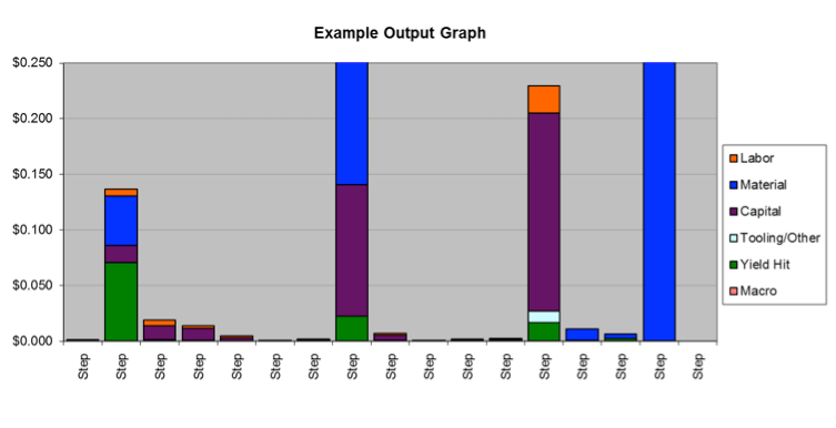
Figure 1 is an excerpt of a graph from our Interposer and 3D Packaging Cost Model. The perspective is zoomed in on a few steps to show how the different cost contributors appear in a bar graph. The names of the steps aren’t specified for this example.
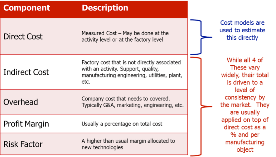
Direct activity costs are not the only costs that need to be analyzed to fully understand the cost of a process flow. There are indirect costs to consider as well, such as risk factor, profit margin, and overhead. The focus of this Knowledge Portal feature is primarily on relative cost changes, so a detailed discussion of direct versus indirect cost is not included. The following chart is a simple way to summarize the different types of cost (Figure 2).
3D IC Cost Drivers
The cost drivers of a typical 3D IC process flow for a two-die stack are summarized below, broken into three categories.
Bottom Die Cost Drivers
- TSV creation process cost
- TSV reveal process cost
- TSV creation yield loss
- Thin wafer yield loss
- Testing/KGD cost
Top Die Cost Drivers
- RDL process cost
- Wafer bumping process cost
Assembly Cost Drivers
- Silicon to silicon process cost
- Silicon to silicon yield loss
- Silicon to substrate
- Substrate cost
At this point in time, 3D ICs are no longer just an idea—there are products on the market. This means that the total cost for some 3D designs is not entirely prohibitive. Therefore, the question to ask is not whether 3D designs are overall too expensive, but in which parts of the 3D process flow is there potential for cost reduction? Of the above cost drivers, which may come down over time?
Immediately visible are a few activities that can be identified as unlikely to change because they are not unique to the 3D IC process and therefore have had a chance to mature already. These would include RDL formation, wafer bumping, and die bonding. Improvements may be made in all three of these areas, but a sharp learning curve and subsequent sharp reduction in cost shouldn’t be expected.
On the other hand, some of these cost drivers are associated with activities only used in a 3D IC process. Namely, many of the activities associated with TSVs (creation or reveal) are new. These have the potential to improve more noticeably.
Example of Cost Changes
Rather than comment specifically on each of the cost drivers listed above and explain why they may or may not be expected to change, a few concrete examples will be examined in more detail. Cost calculations will be carried out to show the changes that may be expected to occur in both mature and not-yet-mature activities, and the impact on total wafer cost will be analyzed.

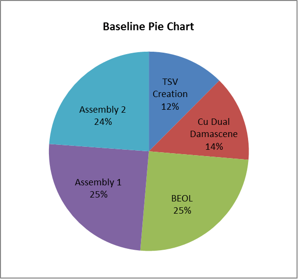
A basic two-die design is used to explore the impact of minor process flow adjustments. The design has a 10x10mm top die and 12x12mm bottom die, and thermocompression die bonding is used. All numbers in this section are a reflection of price, not cost—this means some consideration of overhead, profit margin, and risk factor is taken into account. The following pie chart shows what the baseline results look like when broken down by a subset of steps within the process flow (Figure 2).
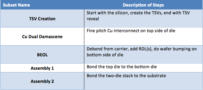
The table below describes what is included in each subset.
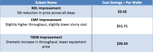
The impact of improvements in three areas is examined: the RDL process (BEOL), a single CMP step (TSV Creation), and the temporary bond/debond steps (BEOL). The improvements in each area are described below, and the table that follows shows the dollars saved in each case.
RDL
RDL creation is a relatively mature process already. There are a variety of ways in which some minor improvements may be seen—lower photoresist prices, improved imaging equipment, improved auxiliary chemicals (developer and stripper). Instead of making a single adjustment in the cost model, the price of the total RDL process (a collection of 22 steps) was improved by 5%.
CMP
The CMP step during the TSV creation is also considered a mature process already. This is a single activity in the series of TSV creation steps in the model, and two changes were made for this example—the slurry cost was reduced by about 27 cents per wafer, and the throughput was increased by an additional 4 WPH. In other words, this example considers the impact of minimal improvements to this already mature process—slightly faster processing and slightly less expensive materials.
Temporary Bond/Debond
This third and final category is the only one that’s not yet mature in this cost example. By making improvements in this portion of process flow, a bigger impact on the entire 3D IC process cost can be seen. For this example, the same changes were made to both the bond and debond steps. The assumption was that the equipment costs come down by a full $1M, and the throughput increases dramatically, by 30 WPH.
In all three categories, the change in price is highlighted—in other words, the amount that can be saved on a per wafer basis is calculated below.
Conclusion
There are clearly opportunities for cost reduction in the 3D IC process. Although an improvement in cost in any part of the process is helpful, the example above indicates that there are certain areas that have the potential for greater improvement. By understanding the cost drivers behind this process, a more thoughtful approach to cost reduction can be achieved.