We’ve heard it expressed many times whenever there’s a new interconnect technology vying for adoption: manufacturers will select the best performing option at the lowest cost to do the job. However, as performance requirements reach previously un-anticipated levels, pitch requirements become tighter, and density requirements become higher, the job of the packaging engineer to provide increased performance at low cost has become more challenging then ever.
Tessera Technologies first launched its wholly owned subsidiary, Invensas Corp. in 2011 to address the challenges faced by today’s packaging engineer. Invensas’ mission was to develop technologies that add value to the package by focusing on advanced interconnect. They adopted the term “Interconnectology” to describe the this focus, and replaced the “packaging engineer” with “Interconnectologist” to better describe the role of their engineers, which called for a combined skillset of wafer processing and packaging. The plan was to hit the ground running with solutions that could be implemented as bridge technologies that meet today’s high-density requirements, while they continued to develop next-generation “Interconnectology” solutions.
 Almost 4 years in, the company has established its interconnect product portfolio. It seemed like a good time to check in with the new company president, Craig Mitchell, who is also CTO for Tessera Technologies, and get his perspective on how the advanced packaging market will play out over the next few years, and where Invensas fits into it.
Mitchell envisions a market where conventional packages exist side-by-side with advanced package-on-package (PoP), interposer, and 3D ICs. “There will be a toolbox of packaging and interconnect technologies, where you pull the particular tool for what you need,” he said. “The market tends to pay for packages that meet the requirements. They will pay for ‘good enough’ with regard to form factor, performance and cost.” While he sees a willingness to evaluate and adopt more expensive technologies, it all comes down to cost and availability of the infrastructure.

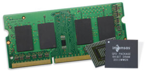
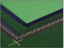
Initially, Invensas introduced its xFD (dual face down) (Figure 2) and BVA (bond via array) PoP as “bridge technologies” that met high-density requirements for memory applications using the existing infrastructure until interposer and 3D TSV technologies were ready for commercialization. Mitchell says they still view xFD and BVA as a bridge from the conventional infrastructure to the 3D IC world, but do not see them disappearing once 3D ICs are in high volume. “BVA fits in very well. It’s a technology that can stay around for many years,” he said. “Packages developed in high volume manufacturing (HVM) stick around for decades. PoP is here to stay for quite some time because it provides an attractive balance of performance, size and cost requirements.”

As xFD and BVA are both memory solutions, I asked Mitchell how the introduction of high bandwidth memory (HBM) and hybrid memory cube (HMC) products that both implement stacked die with TSVs would affect their market share. He said he sees both technologies (HBM and HMC) occupying the higher end of the market, where their higher performance and lower power benefits are required. “xFD is focused on servers more broadly, and there will be some overlap in the high-end server space, but the question is, what can you afford?” he explained. While he expects HBM and HMC to gain traction in the high-end server market, “if you’re looking for a lower cost solution that leverages the existing manufacturing infrastructure, then xFD delivers.”, In addition to high-end servers, Mitchell says xFD offers space savings and higher density in the notebook space. xFD is not yet in volume production, but is transitioning from evaluation to production with working samples in the hands of manufacturers. “We’ve got an agreement with Micron to cooperate on xFD,” he said. “We hope to see products in the market in 2015.”
BVA is a PoP solution to combine logic plus memory, so Mitchell doesn’t see it as competitive with HBM or HMC, but rather provides a less expensive alternative to interposers for vertically integrating logic on memory in smartphones and tablets. “BVA employs the existing infrastructure while increasing the number of interconnects from the logic to the memory,” noted Mitchell. “It’s a packaging solution that allows for separate functions to be stacked vertically using the existing wire-bond infrastructure.”
While technology “chokepoints” are being overcome in interposer and 3D IC devices, Mitchell says cost is still a significant challenge to HVM for these products. “It’s not enough to just be able to perform processes or build structures, you have to be able to build those structures in a cost effective manner to gain widespread adoption,” he explained. Invensas defines HVM according to the ITRS production definition of 20K wafer starts/month. Depending on the die size that translates to 6-7M units/month.

So while companies like Amkor, GLOBALFOUNDRIES and Micron declare these technologies to be production-ready, Invensas is still pursuing solutions that are more cost effective. For example, temporary bond/debond processes represent significant cost, so Invensas is working to eliminate the need for a temporary carrier altogether. “As costs to build interposer and 3D structures come down, the number of applications that can benefit from the performance improvements and power savings will expand,” explained Mitchell. “There are still opportunities to drive costs out of the overall process.” He added that Invensas is also investigating opportunities to improve thermal management techniques. Some can be done with smart design and layout, some with software and how the devices themselves are managed and controlled.
In addition to BVA and xFD, Invensas has advanced interposer 3D IC products in its portfolio. Mitchell says at this time, these are still being actively developed and are at the prototype stage. “We are building out our capabilities, but have not actively pushed the technology into the market yet,” he said, adding that there is no specific timeline, but they expect to have a specific implementation to launch it. They are watching the pick-up of interposer technologies closely, and expect there to be opportunities beyond FPGAs, which combine microprocessors with memory. As cost comes down, interposers will proliferate to other markets, explained Mitchell, but it will be some time before it hits real HVM cost requirements for smartphone applications.
Mitchell says Invensas is also looking into ways to integrate active components into interposers as a way to approach the cost challenge, but that this will be developed in collaboration with a customer to create customer-specific ‘designer interposers’ if you will.
“At the end of the day, we see ourselves as a leader in advanced packaging interconnect technology, and we’re going to continue to focus on next-generation technologies,” said Mitchell. In the short term, he says the company is focused on rolling out xFD and BVA and enabling the infrastructure. Interposer and 3D IC technologies are a key area of focus of the company’s development activities. The ultimate goal is to provide a toolbox of packaging and interconnect options as value continues to shift to packaging to meet the balance of performance, functionality and cost. ~ F.v.T.


