


Despite efforts to leverage the one hour time difference from Phoenix to San Francisco to my advantage, I arrived on the scene at the 2014 3D ASIP Conference to find the morning Pre-conference Symposium on (Interposer) and 3D Design Tools and Flows already well underway. My absence did not go un-noticed by the first presenter, Bill Martin, E-System Design, or by the session organizer and fellow 3D InCites blogger, Herb Reiter. So while there may be a slight hole in the morning coverage, I refer you to the latest musing on 3D By Design by Martin, as well as last week’s contribution on the importance of packaging PDKs by John Ferguson to make up for my absence. The morning session focused on design tool advancements from E-System, Cadence, Ansys, and Mentor Graphics, as well a talk on the benefits of interposer-based System-in-Package (SiP) designs from Zafer Kutlu, GLOBALFOUNDRIES. I will rely on Herb to fill us in on these, and my coverage picks up with the final three presenters, who provided context by offering the customer perspective.
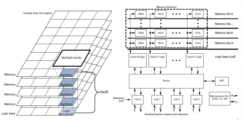
Rambus’s Ming Li built a compelling case for the adoption of 3D TSV for memory applications by first reviewing the traditional wire-bond based packaging, and then comparing it to the advanced interposer and 3D stacked memory solutions that are implementing TSVs such as Wide I/O 1 and 2, High Bandwidth Memory (HBM) and the Hybrid Memory Cube (HMC). LI essentially summarized 200 pages of memory specifications in 20 minutes, highlighting the HMC Specification 2.0 that was just published last week (Figure 1).
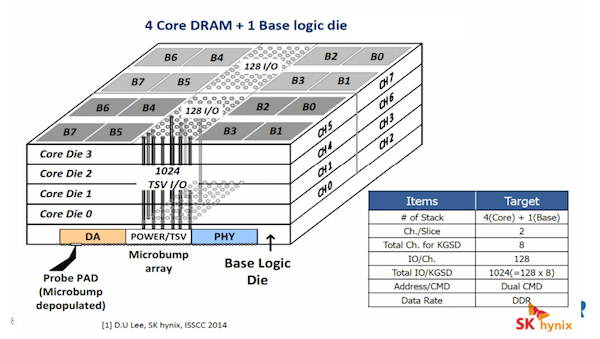
However, the balance of his talk focused on HBM, with an explanation of the HBM overall architecture, which comprises 4 core DRAM die and a base logic die built using a chip on wafer (CoW) approach, and micro-bumped for Si interposer assembly with direct probe pads (Figure 2).
Li said HBM interposer-based applications include CPUs for high performance computing applications, GPUs for graphics applications, and NPUs for network applications. Rambus has conducted Si interposer design studies. Li noted that in a routing study, it was determined that HBM applications need two routing layers. Additionally, due to an electrical performance study, interconnect must be optimized for HBM applications.
Contributing the Qualcomm perspective was Durodami Lisk, who explained that the current gap in the design infrastructure – the lack of Si-package co-design – is not just an interposer/3D problem – but a 2D problem as well. “Closer silicon and package interaction precipitates more robust co-design methodologies,” he said. “Design flow is a critical piece for new technologies. Closer interactions between Si and package are needed for finer lines and pitches.”
Lisk described two approaches to designing across boundaries in which the industry engages: a segregated approach where we do as little as possible to rock the boat and keep lines of demarcation; and an integrated approach, where we jump in head first and blur the lines as much as possible. He also described a hybrid approach where a delicate balance is achieved based on different aspects of design. Lisk stressed that the “wait and see” approach, where EDA houses wait for adoption before investing in tool development, just drags out deployment. Rather, he would like to see EDA partners get involved in co-development work early to ease the path to adoption by reducing “design anxieties” and influence a shift from the segregated approach to the integrated approach. “We need to break this mold and seriously address this from the ground up, especially since this is also a 2D problem!” he said.
A discussion on the importance of power modeling for 3D design, lead by Jerry Frenkil, Si2 – which stands for Silicon Integration Initiative – concluded the design and tool flow portion of the pre-conference symposium. Frenkil described Si2’s efforts and results in developing and standardizing IP and system-level power modeling capabilities, and explained why these capabilities are essential for analyzing power and thermal behavior of 3D designs in real-life scenarios.
Frenkil explained that the power issue for 3D is more complicated than in 2D architectures, because we’re dealing with more transistors in smaller volume with inter-die effects. While we see improvements in energy consumption, energy density goes up. This can create problems with junction temperature and power delivery, he explained. “If we can’t measure it, we can’t improve it,” said Frenkil.
The 3D power challenge, as described by Frenkil, is a temperature vs. power issue. The package is determined by power and temperature, the temperature is determined by the package and the power. Power-related 3D design tasks include thermal-aware floor planning, power delivery planning, and power and thermal signoff. The big issue, he said, is that although the package must be designed early on, reliable power and thermal analysis can only be done late in the flow. “3D design requires early and accurate power analysis for making reliable and cost-effective package decisions,” said Frankil, which is why he said Si2 is calling for standards for system-level power models. Model standards will increase interoperability, increase quality, and decrease cost of 3D design. Si2 has been engaged in developing and standardizing power modeling innovations that can either stand on their own or contribute to other standards.
Wednesday afternoon’s Pre-Conference Symposium session, 3D integration, 3D process technology, whet our appetite for what was to come over the next two days by providing a great re-cap of the industry’s progress in optimizing manufacturing processes that have carried the industry to the point where high-end computing applications are implementing interposer and 3D stacked ICs for memory applications.
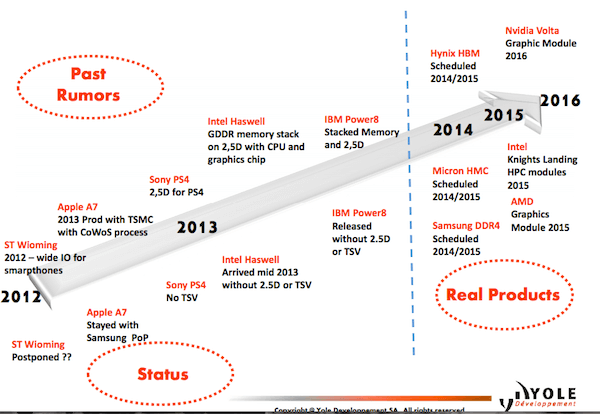
Phil Garrou, presenting on behalf of Yole Développement (with a little of his own personal commentary tossed in for good measure) updated us on the market. I had recently heard his presentation at GIT 2014, and even in that brief period of time he had a few new developments to report. In addition to the now well publicized “real products” from Tezzaron Semiconductor, Samsung, Sk Hynix, and Micron (Figure 3); Garrou topped it off with an exciting bit of news from the HPC world.
First, Fujitsu announced that the Japan Aerospace Exploration Agency (JAXA) has ordered a 3.4 Petaflop supercomputer that will use the latest SPARC64 processor with HMC. Full-scale operations are expected in April 2016. This joins previous announcements of HMC implemented in HPC applications in Intel’s Knight’s Landing Xeon Phi HPC CPU module due out in 2015, and Pico Computing’s 2013 announcement of HMC in its EX-800 blade server for HPC.

The remainder of the afternoon sessions focused on the 3D technology process flow, with Alan Huffman, RTI International, focused on TSV formation: drilling and filling, Severine Charamy, CEA Leti, addressing temporary bond and via reveal, and concluded by Laura Mirkarimi, Invensas, who talked on the little-discuss topic of 3D assembly.
In his focus on TSV formation, Huffman pointed out that the implementation of TSVs for interposers and 3D ICs is different, and that although process steps are similar, there are many different materials involved. He provided a detailed overview of the via first, mid and last approaches, and said that for 3D ICs, via mid has become the de-facto standard. He also talked about solutions to some ongoing technology challenges with TSV fill, including Cu protrusion and overburden removal.
Cu protrusion is a permanent swelling of the TSV surface due to heating. Huffman said TSMC has solved this issue by doing a stabilization anneal step, typically at 300-400℃ prior to processing subsequent layers. He also talked about a low overburden electrochemical deposition (ECD) fill process optimized by Applied Materials that limits chemical mechanical planarization (CMP) time and cost. Huffman also provided a glimpse at forward-looking TSV trends, such as further scaling of TSVs that will mean higher aspect ratios that could challenge current deposition and fill methods. He also talked about competing approaches to TSV, such as silicon-less interconnect technology (SLIT) developed for FPGA integration on a 4-layer 65nm interconnect, but eliminates TSVs and all Si. This was presented by Xilinx and SPIL at IMAPS 2014.
Cheramy provided a comprehensive overview of the various processes and materials that have been designed to address that proverbial fly in the 3D ointment – thin wafer handling. She pointed out the various advantages and disadvantages of a plethora of temporary bond/debond approaches that rely on thermoplastics, thermoset or photoset adhesives; as well those of the carrierless approaches (Taiko process, electrostatic chuck and polymer molding). Which process/tool approach to take depends on each application.
In her effort to provide a full scope of information on the processes she was charged with, Charamy gathered data provided by vendors, as well as from processes worked on at Leti with its partners. With regards to the debate between wet or dry etch for TSV reveal processes, Charamy said that the industry has so far standardized on dry processes as existing equipment sets can be leveraged, making it the more likely path. However, she says she is impressed by the data provided by SSEC and Sachem on its recent inroads in wet etch processes with non-KOH or TMAH based solvents. The companies report achieving <1% total thickness variation (TTV), and that theres is no need for either CMP and cleaning post grinding.
Charamy said if the SSEC/Sachem wet etch process can eliminate costly CMP it would appear to offer a considerable cost savings over dry etch processes. However, she said can’t speak to it personally as they have not worked on wet etch processes at Leti. Rather, work at Leti has focused on via reveal with its equipment partner, SPTS. The objective was to etch a few microns of Si without impacting SiO₂ TSV isolation. They achieved <3% total thickness variation (TTV) on a 300mm wafer.
In her update on Invensas approach to interposer and 3D IC assembly, Mirkarimi talked about select process flows to preserve the µbump interconnect. She also focused on subsequent processes of flux cleaning, underfill and molding. While the rest of the industry has turned to process and material innovations such as Cu pillars, thermo-compression bonding, and self-fluxing pre-applied underfill to address the fine-pitch, low-stand off and high density requirements that come with assembling interposers and 3D memory stacks, Invensas is intent on wringing every last bit of usefulness out of the tried-and-true dip flux and capillary underfill processes and materials that have long been the workhorses of the flip chip world. Mirkarimi talked about the necessity of flux cleaning, and a novel pumping system that is increasing the life of capillary underfill. The company seems to have made it its mission to leverage the existing infrastructure to find low cost solutions that will bring the cost of interposers and 3D stacked ICs down to commodity pricing.
And that was just the pre-conference symposium! Wait until you see what was discussion at the full conference, which took place over the next two days. Stay tuned… ~ F.v.T.


