Like the previous 10 years, RTI International held the 11th 3D-IC focused conference in early December. Instead of the usual two and a half days, this year it spanned 3 days, because it also offered a 4-hour session about 3D design challenges and solutions available from foundries, EDA and IP vendors, a power-user’s 3D views, as well as a low-power design tutorial presented by Si2’s Jerry Frenkil.
Included in the registration fee was also a hand-out with all the presentations and a color softcopy, describing on 66 pages features and benefits of Interposers and 3D ICs, the currently available tools, products and services offered by a broad range of 3D EcoSystem supporters, design examples as well as pointers to 3D books, conferences and other relevant news. If you didn’t get a chance to attend the 3D ASIP conference, the proceedings for the entire conference and the Design Guide can be downloaded at the proceedings tab on the conference home page.
As we reported in previous blogs, IC designs that are destined for production rely on EDA tools to walk the fine line between under-design, causing reliability problems, and over-design, resulting in excessive unit cost and reduced profit margins. This fact motivated about 60 design and manufacturing experts to attend this 4-hour EDA session. They loudly voiced their comments and questions after the individual presentations. I enjoyed very good support from most EDA vendors and other important 3D EcoSytem partners, when I asked them to contribute to the EDA session and to the Design Guide — the supply side is also in full swing.
In addition to reading my observations at this 3-day conference, feel free to also check:
– Francoise’s coverage of the afternoon session of the pre-conference symposium and her takeaways from the full conference.
– Paul McLellan’s observations about the first day of the conference here.
– Jeff Dorsch’ 3D ASIP conference report titled appropriately “It’s complicated” .
I have attended many 3D IC company meetings as well as Interposer and 3D IC focused conferences. Following the presenters’ messages, listening to the audience’ questions and discussing with IC design- and manufacturing experts during the breaks, allows me to say with confidence: The number of companies who aren’t on board the “3D IC train” yet, is getting smaller and smaller. The ones still standing on the platform have valid reasons, e.g. decided to utilize their limited resources for, in their eyes, better things, or address a market segment that’s unlikely to benefit from this technology in the foreseeable future or simply are too busy with immediate revenue generation to jump on board at this time.
Based on my experience with introducing innovative technologies, I expect many of these “currently observing companies” to turn into sprinters soon and jump on board of the moving train. Allow me to name of few passengers, comfortable sitting in a first-class compartment of the 3D Train:
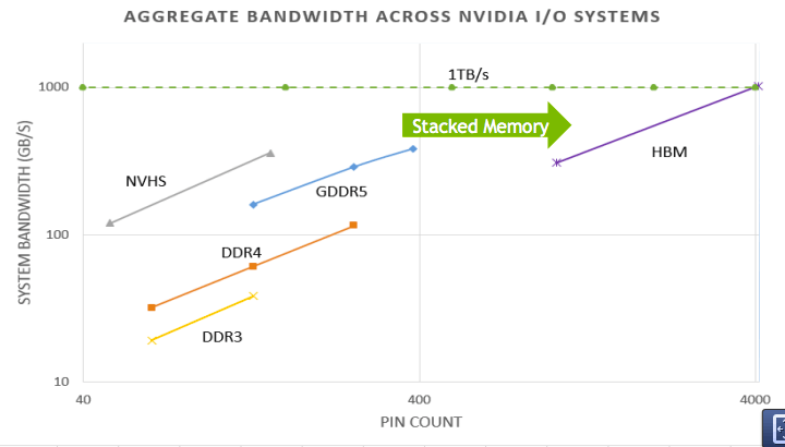
- Alok Gupta presented at this conference how four High Bandwidth Memory (HBM) cubes, surrounding their GPU on an interposer, allowed Nvidia to achieve a bandwidth of 1 TeraByte/second. As comparison: Their previous bandwidth ceiling was 384 GigaBytes/second, when using GDDR5 memories, and consumed significantly more power (Figure 1).
- Xilinx also earned a comfortable seat in a first-class compartment with their 2012 introduction of an FPGA with truly revolutionary complexity. Xin Wu reminded us at the conference that Xilinx had redesigned the FPGA floorplans to combine multiple FPGA slices, arranged side-by-side on an interposer. Xilinx not only enjoys higher yield by partitioning very large design into smaller building blocks, but this modularity concept also allows them heterogeneous integration, e.g. combining dies with FPGA fabric and dies with SERDES circuits in one package. Lower die cost, shorter time to market, lower power dissipation and of course much greater flexibility are key benefits Xilinx can enjoy now.
- Micron’s Robert Sturgill talked about the Hybrid Memory Cube and Novati’s Jeff Wetzel presented Tezzaron’s vertically stacked DiRAMs, both praising the very compelling bandwidth versus power advantages of 3D ICs.
Who else has already taken a seat in the “3D Train” and fully support this new technology?
In addition to many component-level presentations, the conference also addressed system-level topics: The keynote delivered by Si2’s President and CEO, Steve Schulz, highlighted the importance of standards and why Internet of Things (IoT) devices require the ability to combine heterogeneous functions. Logic, memory, sensors, analog, RF, even energy harvesters and power management circuits won’t fit on a single SoC die. These functions need to be combined in a small form-factor, can only zip very little energy and need to be low cost. For meeting these and other IoT requirements interposer- and/or 3D IC solutions should be considered. View Steve Schulz entire keynote below:

Samta Bansal, the former 3D-IC marketing expert at Cadence, now works in GE’s IoT division. Just like Steve Schulz emphasized, Samta also demonstrated the importance of IoT. Consumer products, like Fitbit and Apple’s iWatch, are no longer her focus. She used movies to demonstrate the benefits IoT devices will bring to industrial applications and the smart home in a very compelling way. Samta also addressed the importance of IoT data security and the need to protect embedded software from malicious modifications and copying by an unauthorized entity. Anti-fuse technology provides good solutions for of these challenges.
Other presenters addressed many more interposer and 3D IC related topics, outlined the state-of-the-art in design and manufacturing, including a number of challenges that are being addressed or scheduled to be resolved soon, and even showed how different cost elements impact total unit cost.
In closing, just one more point: Several presenters emphasized that new 3D IC design tools (e.g. Pathfinding as well as PI and Si tools) are also very helpful for designing cost-effective “2D SoCs”. Likewise, manufacturing challenges (e.g. thermo-mechanical interactions) need to be resolved for both 3D ICs and complex 2D designs, to assure reliability. Investing in 3D Technology clearly offers, in addition to a comfortable seat on the 3D Train into the future, also instant benefits for design and manufacturing of 2D SoCs. ~ Herb