


The news about 3D readiness just keeps getting better. Last week I tuned into a GLOBALFOUNDRIES webcast, featuring speaker Rama Alapati, Director
Packaging Engineering, GLOBALFOUNDRIES. Alapati spoke for an hour about the companies’ approach to interposer and 3D integration technologies, and how the open innovation approach has allowed them to develop the critical partnerships with EDA vendors, OSATs, design houses, and customers that have brought them to design-in-ready status for both interposer and 3D ICs. He also highlighted some of the technical hurdles GLOBALFOUNDRIES has overcome so that they will be ready for high volume manufacturing as we transition to 2015.
He talked about the usual drivers: SoC partitioning allows for cost optimization by splitting die on advanced mobile devices. The smaller die size increases the yield, and functionality is optimized. Alapati said GLOBALFOUNDRIES has partnered with Open Silicon to develop SOC partitioning.
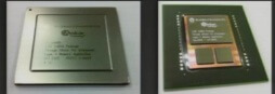
The company developed its TSV process capability in its Malta, NY 300mm fab on 20nm and 14nm. devices based on classical via-mid approach. To date, the company has a reference flow in place, and has developed two logic-memory interposer test vehicles. Both of these vehicles were fabricated at GLOBALFOUNDRIES’ Singapore facility, and they are both named for deserts: Atacama and Kalahari (Figure 1). Atacama was developed as an initial internal test vehicle for tool/line set up. Investigation was based on interposer design and processing, and supply chain set-up. Kalahari is the technology baseline qualification test vehicle for chip-package interface (CPI) qualification and final inputs to defect management (DM) and the process design kit (PDK).
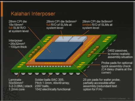
“Kalahari mimics a real system that’s going to be built,” explained Alapati. “We have high confidence that we can take any 28nm technology in 2.5D very fast.”
Talking about the challenges encountered along the way, Alapati said that warpage was the most significant because it caused process defects such as peeling. “We optimized the liner process and the anneal, and now we see no difference between the warpage coming into the module and leaving the module.” He added that they are achieving 98-99% yields and are confident that Si interposers are a high-yielding product. “There are multiple ways to improve the yield, such as adding more TSVs per C4 bump,” he said.
Another challenge with yield was related to die size. With large interposer sizes there is a drop off in yield. He said die-to-wafer is “the technology of choice” to drive up yield. He also said that on the assembly side, there is work to be done with large interposers, but small interposer assembly “is fine”.

Alapati says GLOBALFOUNDRIES supplies TSV wafers to two OSAT partners for backside integration. They also source and validate supporting IP. He reports success with TSV integration and characterization on multiple 20nm and 14nm test vehicles. They established a full flow for 3D TSV wafer processing, and have favorable package test data and demonstrated TSV reliability in the package. Production readiness is targeting Q1 2015.
This webcast came amidst a number of news items about GLOBALFOUNDRIES acquisition of IBM’s microelectronics, which includes facilities in Fishkill, NY and Essex Junction, VT. Probably one of the most to-the-point summaries written was by Daniel Nenni, SemiWiki. In a post titled The GF IBM Deal Explained. Nenni shares the highlights of a one-on-one interview with Gregg Bartlett, SR VP, GLOBALFOUNDRIES as well as his opinion of what a good deal this is for GLOBAL FOUNDRIES. He says acquisition of IBM’s ASIC business, IP portfolio, talent pool of 5000+ employees, and 10,000+ patents is “exactly what GF needed” to get into system houses, differentiate in the fabless semiconductor ecosystem, create an “East Coast semiconductor dynasty”, secure their legacy and a “nice investor exit, and essentially “put them in the same league with Intel and TSMC.” All this, and IBM is paying THEM $1.5. Not a bad deal if you can get it.
Next week at IWLPC, 3D InCites will be hosting a panel discussion, “System-level Advantages of 3D Integration,” on which Rama Alapati will be serving as the voice of manufacturing. I’m looking forward to hearing more about what he has to say on GLOBALFOUNDRIES behalf, and its activities in 3D IC. ~ F.v.T.


