


The annual International Microelectronics and Packaging Society (IMAPS) International Symposium has always focused more on advancements in mainstream packaging technologies, and left the emerging innovative processes to its spring event, the International Device Packaging Conference. As such, its speakers generally offered the most conservative viewpoints on 3D adoption. In a refreshing turn of events, this year’s keynotes and panel talks at IMAPS 2014 called for a change in the way we think about packaging as a market sector, and a look at how technology innovations like interposers, 3D ICs, TSVs, embedded die, and advanced wafer level packaging add value to the device.
In their individual keynotes as well as the panel discussion, executives from Qualcomm, Jawbone, Micron, IBM, IPDia, Advanced Nanotechnology Solutions, and IBM noted that the increased cost of scaling combined with the impending explosion in the mobile, wearable device, and Big Data markets, is driving a paradigm shift that requires innovations in packaging to achieve. Part of this shift requires shedding the lowbrow “packaging” moniker for the more prestigious “system integration” term.
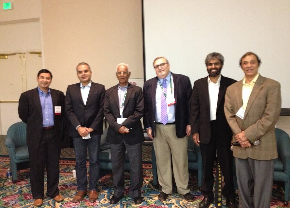
“We are at the cusp of an important transition,” said Subramanian (Subu) Iyer, IBM Fellow, and panel moderator, “We are running out of room on the productivity curve…this is an opportunity that really changes the way we think about packaging.” In fact, Iyer noted that in creating his department at IBM, he purposely called it “system integration” rather than “packaging”.
Rao Tummala, Georgia Tech PRC, the only panelist from the R&D space and a long-time advocate of the term, system-on-package (SoP), reminisced about how up until now, there was no value in the package, and that any new processes or technology needed to be extremely cost-sensitive for adoption to occur. All the value came from the chip. And while that is expected to continue, he said there is also a value-add to a highly integrated multichip package, for which he says we can charge more. Looking 10 years ahead, he envisions packaging being about “making better systems.” Taking “More than Moore” a step further, he offered up “System-level Moore” as an addition to the industry lexicon.
We are in the midst of a “massive wave of innovation” that takes place every ten years, noted Bharath Rangarajan, Advanced Nanotechnology Solutions. He said the rapid growth of the mobile world that “puts computing in everyone’s pockets” combined with “thousands of sensors” gathering data that is collected in the cloud is giving rise to the evolution of systems in billions of little devices. “This is one of the most exciting times in the industry,” he said. “There’s an incredible opportunity at the high end for creating systems that don’t work without the package.” He pointed to the Hybrid Memory Cube (HMC) as an example where integration of memory and logic using 3D TSV technology brings value. Like Iyer, he also objects to the term “packaging” – preferring “interconnect structure”. (This sound familiar doesn’t it? 3D InCites refers to it as “interconnectology.”)
Another example where the package brings value is in wearable devices, where the package is the system, noted Ilyas Mohammed, Jawbone. With wearable product development, “there’s a huge increase in product expectations from sensors and materials to industrial design (ID) and use cases,” he explained. “The component to system boundary is blurred. We’re dealing with a tightly integrated system where every feature and component has an effect.” He said when you start integrating things, issues you have never thought of come up. “What I want from packaging is something that makes my ID job easy. If the packaging is more system-friendly, I don’t have to worry as much.” Moreover, although the semiconductor industry lives “hand-to-mouth”, he’s noticed that consumers are willing to spend thousands of dollars on things they wear every day, such as fashion watches integrated with Jawbone wearables.
While he agrees that we need to get into system integration mode, Steve Bezuk, Qualcomm, says that as an industry we still don’t have the mentality, and there is a huge barrier between designing a chip and then throwing it over the wall to the foundries an OSATS. There’s also the issue of profit margin, where OSATS see 3x less than foundries. Separating the two things doesn’t allow us to pool the advantages of the package, he said. It’s easier for an IDM – even a virtual IDM like Qualcomm – to come up with an integrated solution. “Over the next 5-10 years we’ll still do a lot of classical packaging,” he said, adding that more than 50% of the cost is in the substrate, where there has not been a huge amount of innovation.

Kunal Parekh, Micron, brought his perspective on the topic from the memory market, where increased cost of lithography for scaling is taking its toll, and as such is the next place where 3D IC is expected to ramp into volume production. “When you talk about a $250M litho tool that works some of the time, you start to look at packaging as a solution.” That said, he also sees a world where scaling and stacking die will coexist. People will continue to build multi-billion dollar factories to build DRAM. He predicts segregation between commodity use of memory vs. specific applications, all of which will be driven by applications and system architectures. Memory in the cloud will require both DRAM and non-volatile memory, and will bring in emerging, enabler memories, most of which are 3D devices.
In his presentation, Parekh described the entire process flow of the HMC, and the remaining challenges the industry faces as a whole bringing 3D ICs to volume manufacturing industry-wide. He says Micron and its HMC Consortium partners have overcome and worked through these challenges, and volume production of the HMC is imminent.
“For those of you who think 3D is in the future, you’re wrong,” said Iyer. “3D is in the past. It’s real. Anyone who thinks it’s not happening is in denial.”
This was the very first time at this particular conference that I didn’t hear people say that 3D wouldn’t be adopted until it was cheap as wire bond processes. I call that progress. No longer content to be the “poor cousin” to semiconductor device manufacturing, the packaging community, or should I say “system integration community” is finally fighting for its due. All I can say is, it’s about time. ~ F.v.T.


