
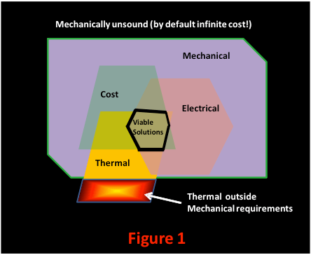
 Fruitful path finding eventually identifies solutions that are viable for mechanical, electrical, thermal, and cost (METC) requirements. Hopefully, more than one viable solution is found to offer a backup in case something was overlooked during exploration or your supply chain can no longer support your needs. Even if you need to re-explore due to changing situations, path finding is still faster and less resource-intensive than performing implementation and verification cycles. Figure 1 shows viable solutions for each METC criteria. The Venn Diagram quickly identifies an intersection of all regions that satisfies all METC criteria.
As path finding is undertaken, each aspect (METC) has negotiable and non-negotiable constraints. Some examples for each aspect are:
- Mechanical:
Non-negotiable: any additional thinning where a wafer is too fragile to withstand additional processing (yields become 0%!). Negotiable is where yields are between 1-99%. Obviously, higher and more stable yields lower the manufacturing costs. - Electrical:
Non-negotiable are insertion loss (IL) worse than -5dB or xtalk (NEXT) levels worse than -25dB that prevent a design from working. Negotiable might be striving for IL no worse than -3dB or NEXT no worse than -35dB. - Thermal:
Non-negotiable for silicon substrate is the operating temperature where the silicon no longer works and models are not characterized. Negotiable could be considered consumer, industrial or military temperature ranges: all viable but with increasing cost.
Cost:
A product has targeted end market(s) that have expected pricing. A cost to manufacture can quickly be calculated from market pricing. This establishes the ‘go/no go’ criteria for cost. Are there exceptions to this? Yes, but if a product radically deviates from the norm, the product needs to have significantly better usability for the consumer. Otherwise, it is a more expensive product that can be substituted by a cheaper but capable product. A recent product that ‘reset’ the consumers’ mindset is the first-generation iPhone: lots of new functionality all encapsulated in a trendy consumable product with a higher price for unit and services than other phones available at the time.
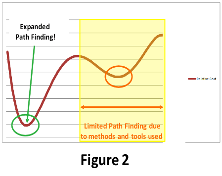 A random walk or a defined exploration?
Random walks can be relaxing but might not achieve an optimum or even a viable product when completed. Exploration based on tools not developed specifically for path finding can quickly cause users to limit exploration due to the increased resources and time required as shown in Figure 2 (shaded yellow). This represents a random walk where local rather than global minimum cost is discovered. As seen in Figure 2, as the path finding scope is increased by using path finding tools and methodologies, a much lower manufacturing cost point is discovered.
Efficient and effective methodology
A defined methodology is needed to help guide exploration. Years ago, a methodology called Design of Experiments¹ (DoE or factored designs) was developed to aid manufacturing lines to optimize their yields and/or performance of their products. I was fortunate to be in an environment where we started to use DoE in silicon manufacturing back in the 1980’s. Prior to this methodology, ad hoc experimentation was used requiring more material and resources to understand interrelationship between variables: often missing detrimental multi-variable interactions. DoE created a structure and helped define the minimum number of experiments that were required to examine multi-variable interrelations. Any person that has worked with DoE realizes how quickly test cases grow based on the required number of factors to be explored. For 9 variables, a 2 Factorial design requires 512 test cases while a 3 Factorial design will require close to 20,000 test cases.² DoE aids planning an efficient path finding by eliminating tests that duplicate other tests. In addition, DoE is effective since it can ensure that all variable interactions can be examined without assumptions or omissions.
Requires tools that are fast and accurate
Regardless of how you have defined your path finding test matrix, many test cases are required to explore how to optimize performance while minimizing cost. Some examples: RDL length, width, spacing, height; via diameter, tapering, length; number of metal layers; oxide thicknesses for via liners as well as inter-metal; etc. Test case construction AND analysis must be fast and accurate for effective and efficient path finding. Otherwise, exploration will be limited by the time and/or resources available. In addition, entire rather than chopped down structures need to be analyzed for accurate results otherwise decisions will be made upon inaccurate analysis.

In summary:
1. Use a methodology to help plan path finding that reduces assumptions and omissions: DoE as an example
2. Choose path finding tools that are: accurate, fast, capable of analyzing large structures and support various materials that are under consideration.
Notes:
1 Many Quality related books discuss DoE. One example: Thomas Pyzdek. “The Six Sigma Handbook”, Chapter 9. McGraw-Hill 2001
2 Bill Martin, Ki Jin Han and Swaminathan Madhavan. “A Path Finding Based SI Design Methodology for 3D Integration.” ECTC 2014 Interactive Presentation.