This week I had the privilege to attend my first Intel Developer Forum (IDF). Like many of us, I have become more energy-conscious, so took the train to get there and back. On my way back I didn’t have to concentrate on the traffic around me and had time to think about what I learned from Intel’s keynotes and Mega-sessions on the first day. For many years, Intel has been the world’s largest semiconductor vendor and one of the few remaining IDMs. How did they manage to get to the top and stay there? I am sure that there are many reasons for it, so allow me to focus on a few of them, to make my point within the scope of this blog.
What impressed me most at IDF, was Intel’s emphasis on partnerships. I checked with IDF Alumni, and they confirmed that Intel always strongly emphasized partnerships at IDFs. This makes a lot of sense, because selling semiconductors is a component business and clearly needs good partners to create useful devices and systems out of these components. Adding other building blocks and software is needed to serve application-specific requirements and generate revenue.
Based on my many years of observing Intel, I have to add: What Intel has been contributing to these partnerships over the years has steadily grown in value, due to including more and more of the peripheral functions around the CPU in their microprocessor. Also, with their reference designs and platforms, Intel has steadily offered more complete and more valuable system building blocks.
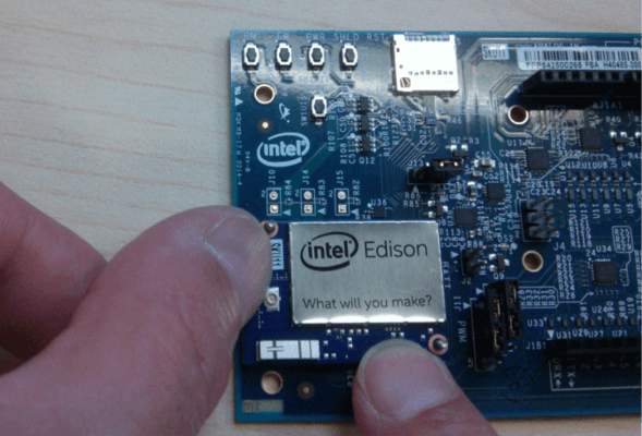
For example, Intel has recently introduced modules on small PCBs, like Edison (Figure 1) to accelerate customers’ system development efforts. What a difference, compared to the big, slow and power-hungry PC add-on cards, which had only a fraction of Edison’s functionality.
Intel is also fully committed to continue following Moore’s Law and announced that they are already working on a 7nm process technology to further reduce power dissipation while simultaneously increasing complexity and speed. Mark Bohr even stated that they know how to succeed in this venture without EUV technology.

Another major effort at Intel is, in cooperation with many partners, the support of the rapidly emerging Internet of Things (IoT). Again, this makes perfect sense, because in addition to capturing revenue from the billions of IoT devices, data centers will rapidly expand and further grow Intel’s revenues in this area.
Intel is also prepared to capture opportunities that require packing heterogeneous functions into a small form factor. Mobile devices and many IoT applications will not only need logic devices, but also large amounts of memory, analog, RF, MEMS and other functions. Due to time constraints I couldn’t attend Sunit Rikhi’s foundry presentation and missed his message about Intel’s 2.5D efforts to address these applications. Intel clearly enhanced their proven multi-die packaging technology to allow logic partitioning and integration of heterogeneous functions in a package. Part 3 of an EETimes article published this week describes a further advanced concept that Intel calls Embedded Multi-die Interconnect Bridge (EMIB). EETimes positions it as a low-cost alternative to 2.5D die stacking. At this time I do not have enough information about EMIB to compare it with silicon- or organic interposers, but I am glad that even Intel has concluded that continued shrinking needs to be complemented with multi-die packaging technology. ~ Herb