


CMOS image sensors (CIS) have often been heralded as the first 3D devices in volume manufacturing. However, this is not really the case. Shellcase MVP, the first generation of CIS that used through silicon vias (TSVs) to form interconnects was still a 2D device. (Remember, TSV is not always synonymous with 3D). Chip stacking only came about with the advent of backside illuminated (BSI) CIS and involved reversing the order of the lens, circuitry, and photodiode from traditional front-side illumination so that the light coming through the lens first hits the photodiode and then the circuitry. This was accomplished by flipping the photodiode wafer, thinning the backside, and then bonding it on top of the readout layer using a direct oxide bond, with TSVs as interconnects around the perimeter. Even then, some don’t consider this a true 3D stack. According to Paul Enquist, CTO, Ziptronix, implementation of true 3D requires using wafer-to-wafer (W2W) hybrid bonding to create “interconnects across the wafer at will without hurting the function of the part.” He said what this means for image sensors is making the electrical connections with the bond without using TSVs, which reduces the pixel exclusion area and allows for increased density.
I caught Enquist’s presentation, and that of Piet De Moor, imec, at last week’s Image Sensors America conference, September 9-11, 2014, at the Hyatt Fisherman’s Wharf, San Francisco, CA. The two speakers comprised the session titled “Stacked Chip Sensors, Is there Any Going Back from Here”? I also caught a few other presentations and quickly realized that not everyone in the image sensor industry is developing 3D stacking technologies, but looking for other 2D solutions to improve pixel resolution.
According to De Moor, this is because many of the companies that were presenting and exhibiting target industrial, scientific and professional markets, and so produce low product volumes. Stacked chip image sensors require high volume manufacturing (HVM) to be cost-effective, explained De Moor, because of the cost of the manufacturing equipment lines. Because of this, to date stacked BSI CIS are only manufactured by Sony and TSMC (for OmniVision) targeting consumer products, where the volume requirements are higher. Enquist also pointed out that Sony is a vertically integrated IDMs and manufactures BSI CIS for use in its own products, and therefore can absorb the cost.
Advancements in 2D Architectures

amp noise. (Image courtesy of Forza Silicon)
In his presentation, Daniel Van Blerkom, CTO, and founder of image sensor design house, Forza Silicon, noted that the consumer market requires a shift from what’s needed for professional sensors. His company’s goal is to bridge the gap between the two markets through the development of a new architecture for high-resolution image sensors that are scalable and can be applied to smaller pixel sizes.
He explained the pitch limitations of large format sensors due to the pixel array and electronics in a single column architecture. Forza’s solution is to break the sensor into multiple blocks of columns (he called it “multiplexing”) to differentiate the signal chain and analog to digital converters, as well as create independent readout blocks (Figure 1). The result is an architecture that can be applied to next-gen professional sensors and consumer sensors. But it’s still a 2D design. When asked about other ways of achieving this, Van Blerkom said, “There is a forward looking way where you could actually stack” but didn’t indicate whether Forza is developing a stacking approach in its design architecture.
The Advantages Stack Up
In his presentation, “Stacking Chip Technology for Imagers,” de Moor outlined an imager integration roadmap in which 2 layer BSI CIS are in production and we “dream of three layers or more.”
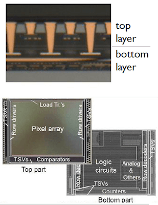
The advantages of two-layer stacks —such as one developed and manufactured by Sony (Figure 2), in which the top layer is the illuminated imager and the bottom layer contains the readout electronics and image processing — is the small form factor, and the ability to stack different CMOS technology nodes optimized for functionality, which is a cost advantage. Another advantage is that wafers can be sourced from different vendors for more options and competition, which will bring the cost down.
Imec and the University of Ghent have collaborated to fabricate three-layer stacks having two layers of CMOS stacked with the imager on top. Moor said this configuration is helpful when you want to not only have the readout on its own layer, but also the memory for on-chip signal processing. This puts image processing like facial recognition, image compression, and depth right on the chip.
De Moor described, in detail, two significant technology “enablers” for two-layer BSI: backside thinning and direct low-temperature oxide bonding from Ziptronix.
He also described W2W hybrid bonding, which combines W2W oxide bonding with Cu-Cu permanent bonding to create high density interconnects, thereby eliminating the need for TSVs and creating the “True 3D stack” defined above by Enquist. Ziptronix has patented this process, called DBI Hybrid Bonding.

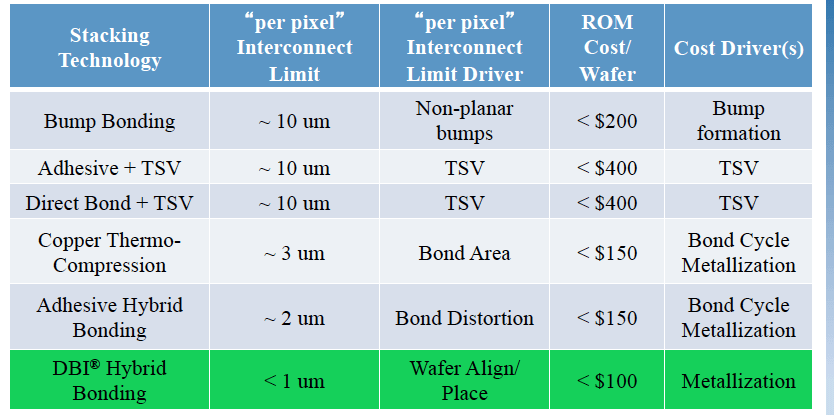
Taking it further, Enquist demonstrated how Ziptronix’ DBI Hybrid bonding is a low-cost solution for stacking without TSVs. He showed the table below as a cost comparison.
The company just announced an industry-first in demonstrating a 3 layer stacked image sensor device in collaboration with Fermilab National Laboratory, to improve the performance of high-end 3D sensor arrays, which are used for particle detection in large-scale particle physics and x-ray imaging experiments.
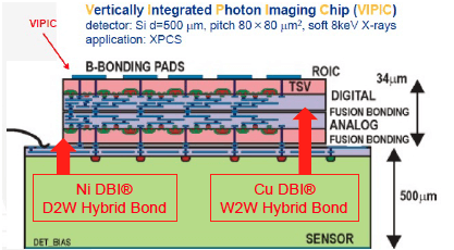
The demonstrator, a vertically integrated x-ray photon imaging chip (VIPIC) detector, was manufactured using W2W DBI hybrid bonding to bond two ASIC wafers containing TSVs. The bonded wafer pair is thinned to expose the TSVs on one side, then singulated. The singulated die stacks are then bonded to an x-ray sensor wafer using die-to-wafer (D2W) DBI hybrid bonding. Subsequent thinning of the other side of the bonded wafer pair allows backside connections to the 3-layer assembly.
“The significance of the Fermilab announcement is that it shows what can be done with this technology, not what’s necessarily next for volume adoption,” said Enquist.
During his talk, Enquist pointed out that stacking technologies for image sensors have been around longer than we realize; since 1977 and commercialized since 1882. He said Ziptronix’ DBI Hybrid bonding was first licensed by Raytheon for focal plane arrays in 2009, and 2012 marked the implementation of Ziptronix’ direct oxide bonding (called Zibond) for consumer stacked BSI image sensors by Sony. (Sony has yet to license the DBI Hybrid Bonding to replace TSV interconnects.)
So If the technology has been available, why the delay in adoption of chip stacking by HVM foundries? “Timing is everything,” said Enquist.“If you consider the history of image sensors, people have been doing 3D in image sensors for decades, but its a matter of going into volume.” He added Sony was successful with its first-generation BSI because the design and the technology were ready. He believes that is just a stepping stone for them. The next step is to build 3D stacks without TSVs, says Enquist, which is one way to accelerate 3D adoption.
“There’s a difference between a technology being manufactured in high volume and being available for manufacture in volume,” noted Enquist. “It’s available but nobody wants to be the first to use it.” All it takes is that first order. And surely for image sensors, chip stacking is clearly a technology whose time has come. ~ F.v.T.


