


3D integration has created a complex landscape of many different package architectures and integration approaches that have diverse materials needs and uncertain insertion timing. The multitude of processes required do not fit neatly into the established pigeonholes of front-end and back-end. Processes such as through silicon via (TSV) fabrication require wafer processing equipment, materials and knowledge to perform, and are generally handled at the fab or foundry. Backside processes that are new to these technologies include formation of front- and backside bumps on the TSV device wafer, temporary bond for thin wafer handling, TSV reveal, isolation and passivation, and the debond step. Depending on the process flow decided upon by the customer requirements, these steps may be performed in the front-end fab/foundry, or in the packaging foundry/OSAT or third-party, such as a wafer bumping house.
In designing materials for this complex landscape, materials suppliers face the ongoing challenge of providing a diverse portfolio of materials to suit the needs of all these new manufacturing process steps, and additionally need to consider process requirements and specifications regardless of where they are performed.
Key Material Challenges
Many of the key material challenges manufacturers face with 3D integration processes, including both interposer and 3D-IC schemes, are highlighted in Figure 1. These include: high-aspect-ratio (HAR) via filling, planarization, fine-pitch bump metallization for both solder bumps and Cu pillars, low-stress/low-cure temperature dielectrics, improved bond/debond adhesives, and new underfills.
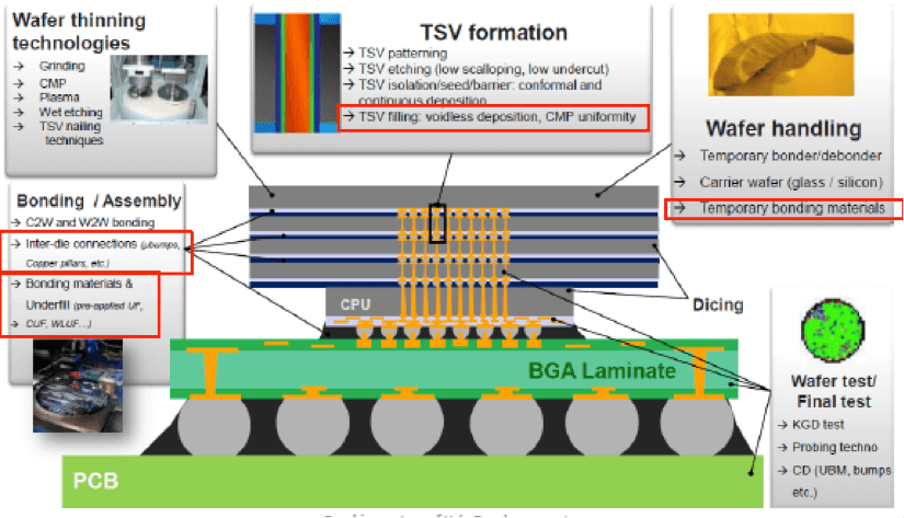
Dow Electronic Materials has been working to establish a suite of materials to enable 3D integration schemes – several will be described here, including metallization chemistries for TSV filling and bump plating; dielectrics for redistribution; photoresists for TSV etch and via reveal steps; adhesives for temporary bond/debond processes; and underfill materials for TSV assembly.
Cu TSV Plating Chemistry
Not too long ago, the industry struggled with via filling process challenges such as mechanical stress due to the coefficient of thermal expansion mismatch between silicon and Cu; additionally, Cu pumping was an issue that often resulted in Cu overburden. Now, the challenges have turned to increasing TSV aspect ratios and I/O density as a way to reduce cost while increasing performance. As a result, new technology challenges have emerged including increased wafer stress, more delicate structures and thinner wafers to handle, as well as difficulties in filling the TSVs themselves. These issues, in addition to efforts to decrease filling times and improve bath stability, all call for optimized plating materials.
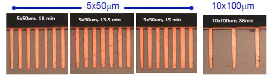
Dow Electronic Materials has designed a Cu TSV filling chemistry for interposer and via middle TSV applications that addresses these challenges. It is a sulfuric-acid-based Cu electrolyte bath with a three-part additive system accelerator comprising an electrocatalyst for bottom-up filling; a suppressor that enhances via wetting and suppresses deposition on field areas and at the top of features; and a leveler that inhibits deposition along the sidewalls and enhances planarization over feature arrays. Performance results for this chemistry include fast filling times and low overburden for a lower cost-of-ownership (CoO). In addition, void-free filling, low defects, high-purity deposit and high reliability/yield have been demonstrated (Figure 2).
Solder Bump Plating
Advanced packaging applications such as flip chip, WLP or 3D-TSV typically utilize lead-free solder joints as a key element of the interconnect structure. The most widely used solder material for these applications is SnAg, which is typically deposited by electroplating due to lower cost and greater reliability as compared to other methods. Bumping processes for 3D-IC devices must be able to address applications with various size bumps ranging from traditional C4 bumps to 20µm Cu pillars capped with SnAg (Figure 3).
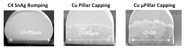
Dow’s offering developed for SnAg bumping and capping is extendable to fine-pitch/TSV applications. Its bath composition is an MSA-based SnAg electrolyte with a three-part additive system comprising a complexer and primary and secondary additives. It exhibits smooth as-plated deposit morphology, tight Ag% uniformity control, achieves within-die and within-wafer height uniformity at fast plating rates for a lower CoO.

Thin Wafer Handling
Handling wafers thinned to 50µm by temporarily bonding them to a carrier wafer prior to backside processing, then debonding afterward is an extremely difficult technical challenge. However, working together with industry partners, Dow has made significant progress in this area. Its temporary wafer bond product was developed for room-temperature mechanical debonding. Based on Dow’s benzocyclobutene resin technology, which is well established in manufacturing as a permanent bonding adhesive material, it has been reformulated to be compatible with wafer thinning and backside integration processes. It features tunable film thickness, low total thickness variation (TTV) for surfaces ranging from low topography to Cu pillars to C4 bumps, and is extendable to fine-pitch TSV applications. Additionally, short cycle time for depositing and curing, coupled with rapid, simple and clean mechanical debonding, results in a lower CoO (Figure 4).

Non-Conductive Films
As new 3D packaging technologies continue to drive to higher I/O counts and smaller form factors, this results in increasingly higher interconnect densities with finer pitches (smaller center-to-center distance between interconnects) and narrower gaps between die and substrate (or between dies in 3D stacked silicon structures). Consequently, it is becoming increasingly difficult for traditional capillary underfill (CUF) materials that are highly loaded with filler particles to flow smoothly and quickly into these narrow gaps (as small as 15mm or less) without resorting to modifications such as vacuum underfilling (which increases process complexity and requires additional tooling) or reducing filler loading (which increases the thermal expansion coefficient, TCE, of the underfill and thereby reduces its effectiveness in managing thermomechanical-induced stresses in the package).
Non-Conductive Film (NCF; also sometimes referred to as Pre-Applied Underfill or Wafer-Level Underfill) belongs to a class of underfill materials that are applied to an unbonded die before the interconnect is formed. Typically, NCF is also a silica-filled epoxy based material except, unlike the liquid CUF analog; the NCF is formulated differently to be supplied in a dry film format. Because the NCF is applied to the die prior to the joining step, this approach is not subject to the same limitations as CUF materials face with regard to flowing into increasingly narrow gaps. NCF materials are therefore a promising approach to extend underfilling processes to advanced packaging applications, especially for 3D stacked architectures.
Dow has developed a silica-filled epoxy-based NCF designed for vacuum lamination on fine-pitch, narrow-gap Cu pillar/TSVs applications. It cures rapidly during thermocompression bonding and results in good bump and fiducial visibility for dicing and alignment. Reliability tests have shown this underfill material to result in void-free bonding without filler entrapment and good joint formation (Figure 5).

Conclusion
2.5D and 3D-IC devices have introduced unique material needs that were not previously required in traditional semiconductor device manufacturing. By developing new products tailored specifically for processes such as TSV Cu filling, Pb-free solder bumping/capping, temporary bond/debond adhesives and underfills for 2.5D and 3D-IC assembly, Dow Electronic Materials is helping to enable the commercialization of 3D integration technologies.


