
Samsung’s introduction of its 3D NAND Flash SSD 850 Pro has led to the inevitable hullabaloo. Amid all the fuss, it hasn’t taken long for someone to publish the actual die size. This of course is the golden nugget of information that lays the foundation for any cost analysis.
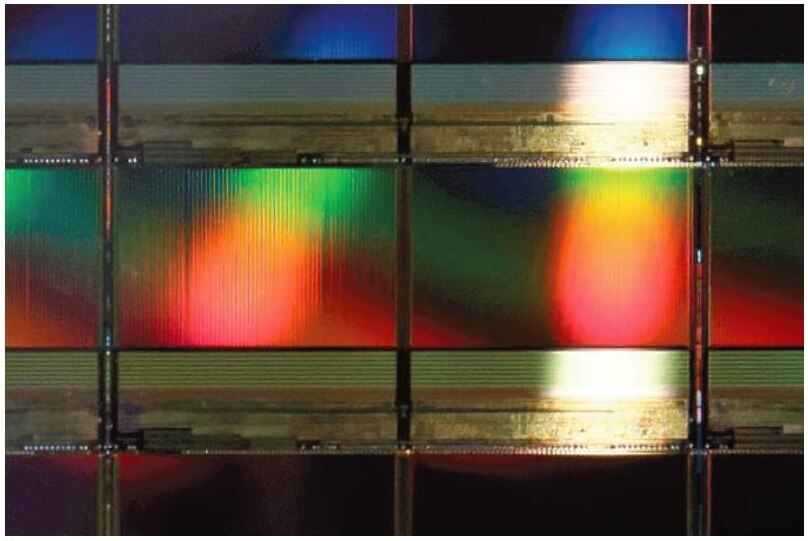
Figure 1 shows a photo, courtesy of PC Perspective, of the actual 86 Gbit 32-layer 2nd generation V-NAND taken on a 300mm wafer.
After a clever piece of detective work on the part of Kristian Vatto at AnandTech, the die size works out to be 6.8mm by 14.0mm giving an area of 95.2mm2.
Samsung had presented in February this year on their 128 Gbit 24-layer 1st generation V-NAND chip which led to my first cell size analysis.
Figure 2 shows the result of a similar analysis using the new 2nd generation data. A comparison of cell size to the 1st generation is shown. The numbers are fairly close but what can be clearly seen is that there is no lateral shrinking.
The assumptions used in this analysis are: 32 layers; 2 bits per cell; no extra cells for other functions; 62% array efficiency (worked out from the die photo). Notice that the array efficiency has dropped from ~80% in their ISSCC presentation.
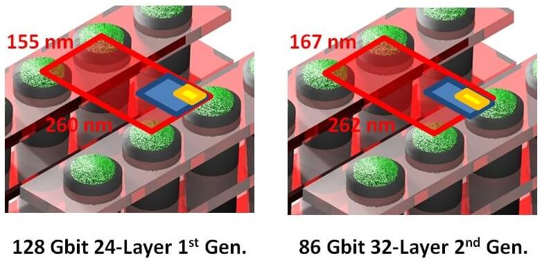
So here we have it. Samsung’s product V-NAND uses a similarly large cell in each layer as their 1st generation chip. Indeed, the cell area worked out on their real product chip is about 33 times the area of Micron’s 16nm cell as given in their ISSCC presentation and reported in my previous analysis.

Maybe that’s why Samsung have quickly gone to 32 layers from their original 24 to give the impression of starting from a similar effective cell size where 2D NAND ends up. Again, congratulations to Samsung for this engineering feat.
However, my skepticism remains as to whether this is a real foundation for future single chip capacity increases towards 1 Tbit. Remember what will need to happen to avoid other solutions undercutting them in cost, namely longer strings and lateral shrinks. And of course good yields. ~ AJW