


I don’t know why it still surprises me to read conflicting reports on the progress of 3D TSVs. But I think Ron Huemoeller, Amkor, finally hit on it in his closing remarks during today’s webcast, “TSV Packaging at the Tipping Point”, moderated by Pete Singer, Solid StateTechnology/Extension Media.
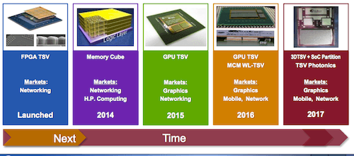
Huemoeller’s presentation and that of David Butler, SPTS, once again reinforced what we’ve been reporting for quite some time on 3D InCites; using TSVs for SOC disintegration reaps substantial cost/performance benefits over continued scaling, (although Huemoeller was emphatic in pointing out that it will not ever replace scaling). Additionally, 3D TSV processes are ready and sufficient yields are being reached (Butler claims that 99% yields have become the norm). Huemoeller showed an updated applications and market roadmap of advanced packaging progression to illustrate his point that with 3D the future is NOW. We’ve already seen 3D TSVs in FPGAs, this year is the year of the Hybrid Memory Cube, and 2015 will bring TSV GPUs.
Regarding thermal management at the package level, Huemoeller says Amkor has been using standard thermal interface materials, heat sinks, and substrate materials during assembly processes to dissipate the heat in GPU packages. “We’ve had to do nothing different to accommodate these multi-die schemes and monolithic schematics,” he reported. “They’re passing package reliability tests and functional tests under performance.” Equipment suppliers like SPTS are now focusing on optimizing tools to fine-tune processes and help lower the cost of ownership. Butler demonstrated as much in his presentation about SPTS’svia reveal process.
“We are at a tipping point in the industry today where TSV has an opportunity to release broadly in many product formats,” said Huemoeller, “It’s all about having the courage to design into it, first and foremost. Some companies are now doing that as they see cost/performance benefits. Other companies will follow quickly as competition heats up and they don’t want to be left behind as they see that the benefits are too great to ignore.” He added that designing in TSV formats will “kick if forward”.
Butler echoed Huemoeller’s optimism. “People are coming up with good reasons for why we have to go 2.5D and 3D,” he noted. “I’m more enthusiastic about the near-term future of this than ever before.” Butler’s presentation explained SPTS’s blanket etch processes, which I discussed with SPTS’s Dave Thomas at ECTC 2014.
In other reports from various online semiconductor news sources, journalists are reporting more mixed stories, where in some cases, mayhem in the industry is finding solutions in 2.5D and 3D architectures, and in others, it’s still not considered to be the answer.
In his post “Semiconductor R&D Crisis Ahead?” SemiEngineering’s Ed Sperling talks about how the myriad of R&D investment choices has many companies paralyzed in indecision, as the next move could possibly make or break the company. Sperling interviewed executives at EDA houses, Synopsys, Cadence and Mentor; as well as fabless design houses like eSilicon, Open Silicon, Synapse Design and others, to find out how to navigate the uncharted waters of too many choices, each with uncertainties.
While he lumped investing in 2.5D and 3D stacking with the list of indecision that includes FinFETS, node shrinks down to a possible 5nm, or “eking more from existing processes nodes by using new process technologies, more compact designs and improved architectures”; he also points to 2.5D and 3D stacking as a way out, because it provides a simpler way to achieve performance needs with existing nodes through architecture vs. investing in future nodes, whose performance is only required for networks, servers, and highly compute intensive applications.The ability to break up larger designs into smaller parts that function independently and integrated is beginning to be seen by system designers as an attractive option.

Reporting from imec’s International Technology Forum in Belgium, SemiMD’s Ed Korczynski predicts that “the future of 3D memory will be in application-specific packages and systems” as 2D scaling reaches atomic limits. And by 3D memory, he’s referencing not just 3D stacked DRAM, such as the Hybrid Memory Cube (HMC) but six different version of 3D NAND. “Nanoscale electronic systems will use 3D memories to reduce volume and signal delays.The future of 3D memories will be complex, but industry R&D collaboration is preparing the foundation to be able to build such complex structures.” It certainly seems that imec isn’t as paralyzed with indecision about where to invest. They will do it all.
Alternatively, in his recent post, Mobile Packaging Market Heats Up, SemiEngineering’s Mark Lepedus writes that while mainstream packaging appears to be “running out of steam” for the needs of mobile devices, 2.5D and 3D ICs appears to still be considered a too-costly option, and is being pre-empted by advance package on package (PoP), fan-out wafer level packages (FOWLP), and embedded die technologies, at least in the mobile market. FOWLP is not suited to high end computing.
Interestingly enough, on the topic of cost, during the webcast, Huemoeller commented on cost, and how Qualcomm set a gate at 1¢/mm², which essentially set the threshold release point to bring TSVs into the mobile market. “We see ways to bring pricing down below that gate.” he said, adding that efforts are proceeding nicely.
So the controversy continues, but at the end of the day, as Huemoeller predicts, it all comes down to courage. We’ll see who has it and who doesn’t ~ F.v.T.


