


Through silicon via (TSV) reveal is a critical part of the wafer-thinning step in 3D IC backside processing, where the wafer is thinned to expose the Cu “nails” that ultimately form the interconnect between die stacks. Some of the risks involved in this step include backside contamination (Cu diffusion) due to premature contact with the vias. Poor via fabrication depth uniformity can also contribute to issues with remaining silicon thickness (RST) post-grind, and may result in nails that are not evenly revealed, and in some cases, not exposed at all. As a result, the TSV reveal step has continued to be one of the more costly due to expensive processes and poor yields.
To remedy these issues, several companies at ECTC 2014 presented different approaches to fine-tuning the steps leading up to and during via reveal. I spoke with representatives of Lasertec and Disco about combined work to integrate feed-forward metrology data to improve the post grind RST. I also talked to representatives from SPTS, SSEC and Sachem about progress being made in dry and wet etch processes for TSV reveal, respectively.
Feed Forward For Uniform Grind
The whole TSV reveal process begins with grinding the device wafer, which has been temporarily bonded to a wafer carrier, to 5-10µm above the TSV. The goal is to use etch processes to remove the remaining silicon to achieve a 50µm thinned wafer with exposed TSV Cu contacts. How the initial grind and post-grind surface preparation is handled can play a part in the final product.
“Via etch, wafer bonding, support wafer thickness variation all affect the incoming wafer before grinding, and have to be considered during the grind process to achieve the most uniform RST possible,” explained Frank Wei, Disco.
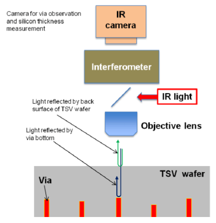
Disco has teamed up with Lasertec to demonstrate the benefits of combining a metrology tool and a grinding module to achieve better results. First, a Lasertec metrology tool measures RST between the bottom of the TSV and the backside surface of the wafer by using IR reflectance to measure total wafer thickness by laser displacement, and measures the thickness of the via using IR interferometry (Figure 1). The tool then feeds forward measurement data to a Disco TSV wafer thinning module that can interpret the data and make changes to the grinding depth within the wafer to leave the thickness of silicon above the TSVs as uniform as possible. The grinder features an adjustable chuck table assembly to achieve a tailored RST profile (Figure 2.)
According to Wei, there are limitations to grinding based on manual calculations due to the variations in the adhesive used for the temporary bond and the central symmetric grind process. “Metrology is critical because we have to make sure the tallest via has Si above it. Feed forward data helps with process control,” he explained. “Without metrology, you’re making a calculated guess and can’t grind as close to the vias as you can with the provided data from the Lasertec tool.” The key take-away from this work is that the feed-forward metrology improved control and variability of the TSV process.
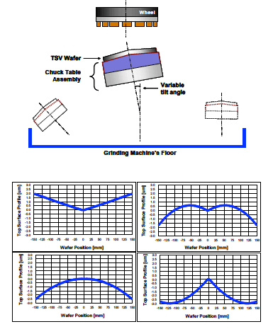
axes of the chuck table with respect to the grinding spindle. (Image Courtesy of Disco)
The two companies implemented this process at IBM in Fishkill, NY on a processed wafer. According to Wei, IBM wanted to develop a product and needed a controllable process that would help in cost reduction and increase control, said Wei. The lower the RST target, the lower amount of reveal to achieve uniform exposed Cu nails. This translates to increased throughput and lower cost of ownership (CoO), he says.
The reveal process step itself can be approached a number of ways. According to Wei, if the end-device is a passive interposer, than Cu contamination is not critical and the Disco grinder can be used to grind the wafer flat to reveal all the vias in one shot. Alternatively, active devices – for example memory die stacks – requires grinding to a calculated profile to leave a layer of Si above. The next step is chemical mechanical polishing (CMP) and cleaning to polish and prepare the surface to be hydrophilic; a process for which Disco also supplies tools. Wei said Disco’s CMP and clean steps are etch-agnostic – it can precede either wet or dry etch. “We work with other equipment vendors to combine modules. It’s not difficult to combine the interface,” he explained.
So depending on the manufacturer’s preference, the via-reveal step for active devices can be performed using either dry or wet approaches. We have covered both extensively on 3D InCites over the past year, and got recent updates at ECTC 2014.
Progress in Dry Etch
According to Dave Thomas, SPTS, the company has been focused on its dry etch reveal process for the past year or so, with an emphasis on improved etch rate and uniformity control. It’s a strategic decision. “The major players are chasing the TSV fabrication business,” he said. “We’re positioning ourselves for backside processes.” 3D InCites recently covered Richard Barnett’s presentation on SPTS’s progress with end-point detection at SEMICON Singapore.
So in my discussion with Thomas, we talked about the company’s work to improve etch rate and the uniformity control through tuneability of the etch process. He reports that over time, they’ve increased the etch rate from 2.5µm/min to 9µm. It is also possible to shape an etch profile to accommodate wafers that aren’t uniform post grind. “If you have a center-thick RST you can do a center-fast etch to compensate,” he explained, for example. He also said that while the company has demonstrated a 1.5µm RST range across a 300mm wafers, that’s based on imec wafers that were extremely flat. “imec is chasing a 1µm tip height. If you can repeat that, it takes cost out,” he said. If companies can control incoming wafer flatness, than a 1µm endpoint is possible.

“It’s staggering at how bad RST control really is out there and the requirement for tuning is huge,” said Thomas. He said typical RST range of wafers coming into the manufacturing environment is anywhere from 2.5 up to 5µm. “We can typically achieve a 2µm range, but it depends on the incoming wafer.” he said. “Concentric distribution within 1-2µm is possible with via reveal etch recipe tuning.” He added that regardless of the incoming shape, end-point detection can be used, but he couldn’t tell me how. That’s SPTS secret sauce.
Wet Etch Progress
With regard to wet etch, over the past year 3D InCites has focused on single wafer wet processing tool enhancements that enable low cost and improved performance for wet etch processes for the via reveal step. At ECTC 2014, we learned about recent advancements in the chemistry formulations thanks to the collaborative efforts of chemistry supplier, Sachem and equipment manufacturer SSEC. Laura Mauer, CTO, SSEC alluded to this work last year at SEMICON West. The goal was to replace tetramethylammonium hydroxide (TMAH), the workhorse of etch, with a chemistry that has a good etch rate, but that doesn’t carry the health issues of TMAH, or the residue or cleaning requirements of potassium hydrochloride (KOH), which is the current substitute for TMAH that SSEC has been using in its wet etch processes.
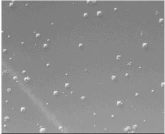
“TMAH has been key for everything from developers to Si etching,” said Yongqiang Lu, electronic applications director, Sachem. “But TMAH has major health issues, its highly corrosive and crosses the skin barrier,” Lu said. Sachem has been exploring alternatives with the same or better functionalities that suit a range of applications. The result is a new chemistry that “fits beautifully.” They began with an alternative quaternary hydroxide molecule that functions similarly to TMAH, with regards to etch rate, but with favorable dermal toxicity numbers. “Through formulation work, by modifying the molecule we can create a fast and smooth silicon etchant. The final reveal surface has no ‘pyramids’ created by anisotropic etch along the crystal planes,” said Lu. (Figure 1).
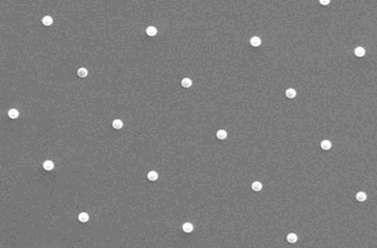
The new chemistry is being commercialized under the name RevealEtch, and was developed specifically for the reveal step. It etches silicon with a high precision rate and a lack of roughness, said Lu.
Mauer explained the two-step process TSV reveal process developed by SSEC, based on Sachem’s new chemistry. It begins with a spin etch using hydrofluoric acid (HF) and nitric acids to achieve a smooth, fast etch. The etch is stopped 2µm above the TSVs and then they switch to a selective etch process using RevealEtch. Mauer said this eliminates the need for CMP or dry polish, so you go directly from grind to wet processes.
According to Mauer, having to use TMAH, with its slow etch rate and high concentration, prevented people from using wet etch, which is a shame, considering the cost of ownership benefits of wet etch for TSV reveal. RevealEtch’s good etch rate, with no potassium residue to clean, and no health issues eliminates the concern. It just might change the way people think about wet etch. ~ F.v.T.


