
Imagine this: aquamarine tints of the Pacific washing sandy Hawaiian beaches amid the balmy breeze and only yards away, several 3D NAND papers being presented at the recent VLSI Symposium in Honolulu. Idyllic!
I counted five papers in total associated with various forms of 3D NAND. The protagonists were: SK Hynix in association with KAIST on one paper and Seoul National University on another; Macronix alone on one paper and with Synopsys on another; and finally IMEC in association with Excico.
While one paper dealt with the troublesome effect of in-process charging and how to avoid it, all others had something to do with the non-crystalline grainy nature of the channel material.
Grainy, polycrystalline channels have such a limiting effect on electrical conduction that two papers looked at how to sidestep this issue. These are the papers I will discuss here since they are valiant attempts to deal with this fundamental drawback of 3D NAND.
If you need a primer on how disordered channels affect electrical conduction in 3D NAND strings, have a quick scan of two of my previous blogs. The key to remember is that vertical channel approaches such as Samsung’s V-NAND and Toshiba’s p-BiCS primarily rely on string lengthening to increase single chip memory capacities. Therefore, channel string currents threaten to decrease rapidly with capacity increases.
The first paper (J.K. Park et al., “Surface-Controlled Ultrathin (2 nm) Poly-Si Channel Junctionless FET Towards 3D NAND Flash Memory Applications”) from KAIST and SK Hynix (nice to see such a collaboration) looks at how to boost channel conduction by thinning the channel thickness. As you may have realized, the area of electrical conduction through a thin-film transistor with a disordered channel is as close to my heart as they come.
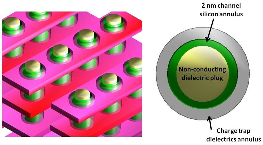
Figure 1 shows how this would look in a vertical channel 3D NAND. The green annulus is the 2nm channel silicon. This surrounds a non-conducting dielectric plug and is itself surrounded by another annulus of charge trap dielectric layers.
Notice how the vertical string has two distinct pieces of channel region: first, the piece aligned with the horizontal gates and second, the piece between the horizontal gates. This paper looks at what happens when the first piece is thinned down to 2nm. I’ll talk about the second piece later on.
Since the channel regions between the gates in any vertical channel 3D NAND cannot be selectively doped to form sources and drains, the channel silicon is usually all doped N-type to improve total string conduction. This then is called “junctionless” or “JL” for short. To avoid high string leakage current uncontrolled by the gates, this N-type channel silicon has to be made thin enough for the gates to have the ability to open and close the vertical channel conduction.
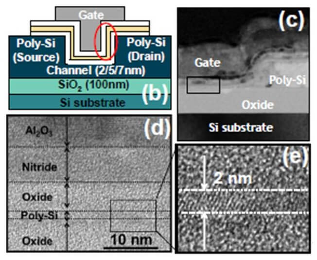
The authors’ motivation for this study is to find ways to maximize the current through such a thin channel annulus for 3D NAND. Their experimental approach is to make standard planar thin-film transistors with 2nm thick channels, shown in Figure 2, and assume that the results will apply in a vertical channel 3D NAND.
Their results are certainly impressive as far as current conduction in very thin channels is concerned. In fact, this may be the thinnest silicon-based channel thin-film transistor to date. The authors show better conduction in 2nm channels compared to 7nm for both JL and IM devices. Congratulations to them for this achievement.
However, there are a number of serious challenges in the path to 3D NAND use. The main one is that a vertical 3D NAND implementation of this will have 20nm channels between the gates in the vertical direction (the second piece mentioned above) which presents a high resistance in the string and where the gate has little positive impact. The experimental device avoids this by having thick, low resistance source and drain regions as shown in Figure 2.
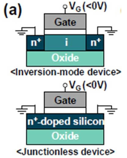
The second challenge involves the electrical activation of the channel dopant or rather, poor activation. In other words, is it really N-type? Figure 3 shows the two types of devices being compared in the study. The JL device has a highly N-doped channel, whereas the “Inversion-Mode” or “IM” device has an intrinsic (undoped) channel. We would therefore expect the JL device to turn on at lower, actually negative, gate-to-source voltages since its channel is already full of N-type dopant atoms. The problem is that it is very difficult to activate dopants in disordered silicon. This is a well-known issue and can actually be seen in the authors’ data where no real difference is discernible between the turn-on of a 2nm JL device and that of a 2nm IM device. In fact, the JL device looks to have a higher threshold voltage. I don’t know if the authors missed this but it means that the classification of devices into JL and IM types is not supported by the data.
What does this second challenge mean for 3D NAND implementation? Well, the ultra-thin channel between the gates in the vertical direction needs to be highly N-doped to lower its resistance. The fact that it is probably undoped will present a high string resistance.
So, in summary for Park et al., very interesting physics, congratulations for record-breakingly thin channels but real challenges remain for 3D NAND use.
The second paper (J.G. Lisoni et al., “Laser Thermal Anneal of polysilicon channel to boost 3D memory performance”) from IMEC and Excico looks at how vertical channel 3D NAND string currents can be increased through the use of laser melting and subsequent crystallization of the channel silicon. The use of laser annealing to crystallize deposited amorphous silicon can be traced back to great work done by J.S. Im in the 1990’s. In Im’s work, the silicon film to be crystallized is a horizontal deposited sheet.

The improvement of thin-film transistor behavior through laser annealing has been used in the flat panel world for over a decade (do a Google search on “continuous grain silicon” from Sharp for example).
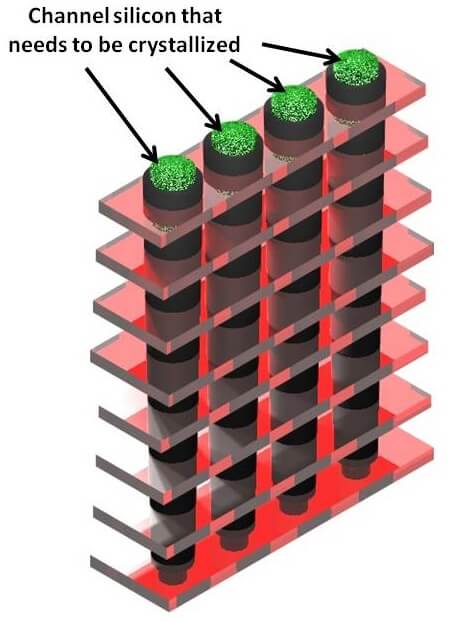
The vertical channel 3D NAND however presents a tricky proposition. Figure 4 shows that the laser needs to melt and crystallize the deposited amorphous silicon all the way down the channel hole without causing damage at the top.
The authors built a single device with a vertical channel (so no string) and found a window of laser energy areal density that maximized the device performance without causing damage. The result is that, on its own, the laser annealing is effective to a depth of about 400nm. To put this into perspective, this would be about 6 cells in a string when the cells have a gate length of 30nm and spacing of 30nm.
To achieve deeper crystallization depths, simultaneous substrate heating during laser annealing is put forward as a solution. This then is simulated to achieve a depth of about 900nm. This would be about 15 cells deep with the cell dimensions mentioned above.
The experimental structure has a channel diameter of about 45nm. I wonder how the results would be affected if this hole were smaller since the melted silicon will have closer critical interfaces that affect final grain size?
The authors achieve about 30-40 times the channel current per unit width (at 5 volts gate-source voltage) compared to the Park et al. paper with their 2nm channel. However, the same question arises as before: what happens in the channel regions between the vertical gates?
In summary, the authors have certainly been able to dramatically improve the single cell in terms of current conduction and transistor turn-on. This is not really all that surprising given what has been done elsewhere. However, its usefulness in the vertical channel 3D NAND space is, in my opinion, not proven in this work. Even with the proposed substrate heating (which I assume will be shown experimentally in a subsequent paper), only a portion of a string can be reached. How would the technique be applied to Samsung’s proposed 192 cell string in a 1 Tbit product?
The VLSI Symposium certainly contained interesting 3D NAND work but, in my opinion, the string current remains a serious concern.
The aquamarine tints and balmy breeze beckon again…. AJW