


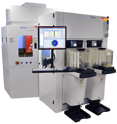
 The TMAP DUAL 3D 300 A is a unique metrology and inspection tool available to the semiconductor industry capable of addressing all customer measurement requirements for MEMS and 3D packaging. The TMAP is highly flexible, accurate, and repeatable. The heart of this tool is based on multi-sensor heads which include different technologies in the same integrated tool. As an example, double IR microscopy is coupled with reflection and transmission IR Illumination. The inspection technology allows the TMAP to detect cracks around the TSV, and inside the silicon layers. Our EFEM is able to handle standard or Semi- Standard products as well as wafer frame in 300mm. FOGALE has a continuing development effort that has tracked and satisfied customer requirements and stays in front of the next production needs.
Testimonial
Customers need a metrology & inspection tool for the 3D IC with the capability to perform, for example, through silicon via (TSV), remaining silicon thickness (RST) and copper pillar height measurements in addition to inspection for cracks, wafer alignment edge control, etc… From a simple interferometer with fiber, FOGALE managed to answer this 3D IC Challenge in a short time, and proposed a 300mm production tool with broadband sensors that provide different technologies and IR microscopy top and bottom. This tool is now able to handle wafer frame 300mm and pass over the current Customer requests for this market. Additionally, we are always happy to receive new customer requests in 3D IC and propose to demonstrate our technology knowledge at any time.
- Fogale Website
- Date this Product was Introduced to the market: 9/2013
- Category Product is Being Nominated for: Inspection/Metrology Tools
- Technical Information for the TMAP Dual_3D 300 A


