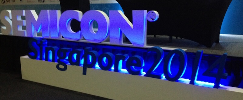
 This week, at the invitation of SEMI Southeast Asia, I made the monumental trek from Phoenix, AZ to Singapore to attend SEMICON Singapore. While I know many of my industry colleagues make these journeys in the regular course of business, this was a new experience for me and my first visit to both Singapore and SEMICON Singapore, which has historically been focused on the packaging, test and assembly segment of the semiconductor manufacturing market due to the number of OSATs located in Southeast Asia. I can say without a doubt, that the experience has been well worth the trip.
This year’s program (and the main reason for my presence) included an all-day 3D IC Forum, chaired by Surya Bhattacharya, Ph.D. of A*STAR Institute of Microelectronics, which turned out to offer a refreshingly optimistic perspective on the progress of 2.5D and 3D ICs, in comparison to last year’s 3D IC Forum. Last year, presentations focused on the need for lowering the cost of 2.5D and 3D, and looked for alternatives to TSV. This year, while cost reduction is still on the to-do list, it wasn’t identified as a show-stopper. Rather, because cost is an issue, actual solutions were presented by equipment and material suppliers Tokyo Electron, Attotech, EV Group and SPTS, who have focused efforts to optimize processes to lower cost. Additionally, rather than alternatives to TSVs, presentations from Rosalia Beica, of Yole Developpment, Yoon Seung Wook, Director, STATS chipPAC Ltd., Sitaram Arkalgud, Invensas, and Battarcharya, IME all talked about the suite of technology solutions, from fan-out WLP, embedded die packaging, 2.5D and 3D ICs to address today’s package requirements.
Jan Vardaman presented a 3D market update slide that finally doesn’t push adoption much further out, but rather remains fairly consistent with last year’s prediction of 2015-2016 for 2.5D adoption for GPU plus memory stacks on interposers and the start of networking applications. While the chart is not yet available for publication, Vardaman noted that less than 20K interposer wafers and less than 10K 3D IC wafers will ship in 2014. By 2017, we can expect to hit the 1M wafer mark for interposers, and 352K 3D IC memory wafers by 2018.
“We are getting 2.5D and 3D ICs into production,” noted Vardaman. “but we don’t see a lot of volume happening until 2015.” Breaking it down by device, she reports that in 2015 we’ll see GPUs next to memory stacks on an interposer. 2016 will start bringing interposer and memory stacks to networking applications, followed by servers and potentially tablets.
Vardaman also noted that since she presented her industry ‘report card’ back in December, progress has been made in a number of areas where she had given poor grades, namely improvements in test areas, design, and in temporary bond/debond (TB/DB). She still expressed concern about a lack of commercially available thermally-aware design tools to solve thermal issues, but has amended this concern to be in cases where where logic is part of the stack.
From the volume manufacturing perspective, the outlook for commercialization appears quite rosy. Ramakanth Alapati, Senior Manager, Package Architecture and Customer Technology Group, GLOBALlFOUNDRIES and Dr. Yoon Seung Wook, Director, STATS chipPAC Ltd. indicated manufacturing readiness for 3D TSV when the customers call for it.
Even though Alapiti’s presentation was titled “Sub-20nm node 3D IC Packaging Challenges,” the overall message of his talk was that at GLOBALFOUNDRIES, these challenges have been addressed, from the TSV process flow, temporary bond/debond, thinning, and keep-out-zone (KOZ) issues; to permanent bonding, chip-package interconnect (CPI), thermal management, and the supply chain.
“(At GLOBALFOUNDRIES) there are no showstoppers anymore,” said Alapati, in an interview following his presentation. “We can design and process around what challenges remain, even thermal. Materials have come a long way. Designs will naturally progress. We know how to control thermal performance through big.Little architecture.” (Big.Little architecture is ARM lingo meaning big processor with small power management to manage the performance.)
I asked about the TB/DB issue that many still cite as one of the remaining showstoppers. Alapati said that for GLOBALFOUNDRIES, TB/DB is well understood, and noted that OSAT partner, STATS ChipPAC has very credible data. Access to the latest tools have allowed them to make a lot of progress over the past couple of years. He said its a matter of running a couple of hundred wafers and having very accurate yield tracking to monitor the performance. Companies still struggling with this issue may not have access to the latest HVM equipment, he added.
Alapiti explained that GLOBALFOUNDRIES open supply chain approach allows existing and future customers to keep their existing supply chain. “We have JDAs with all four major OSATS, and have test chips in all of them for a smooth product map.” he said. They partner with design firms up front to establish the design flow, rules and tool alignment. Bump and probe is a customer choice, and the back-end processing depends on the OSAT capabilities.
“Our 20nm technology is ready for prototyping and HVM,” said Alapati. “All the critical TSV, thin wafer handling, and die stacking technology challenges are well understood and over come with our collaborative supply chain model, and we are ready to take orders next year.”
Alapati says he thinks that there will be a push to 3D ICs in consumer mobile products much sooner than 2018 to maintain a performance edge in mobile end product. “2015 might be the year products are shipped in 3D in the mobile market,” he said. He also said that while GLOBALFOUNDRIES is focusing on 20nm and 14nm nodes for 3D, what nodes the first products come out in may surprise us; it may be 65nm node.
Just because GLOBALFOUNDRIES has it all figured out, doesn’t mean the challenges don’t still exist for others. But nonetheless, Its exciting to hear such a positive message from such a key industry player. It certainly bodes well for the future of 3D. ~ F.v.T.


