


Customers have asked and suppliers are listening. One sign of progress from last year to this year at SEMICON Singapore’s 3D IC Forum was the number of supplier presentations focused on process improvements that have been developed to lower the 3D IC cost of ownership (CoO). In addition to the cost-effective implementation of interposer technologies being worked on at Singapore’s A*STAR Institute of Microelectronics and Invensas Corporation, which I discussed in a blog post yesterday, other inroads into cost-saving measures included a via-last approach combined with temporary bond/debond improvements from Tokyo Electron; a controlled via reveal process from SPTS; and several solutions for low-cost filling processes for interposer through silicon vias (TSVs) from Atotech and EV Group.
In his presentation titled, 3D IC Equipment and Process Challenges and Solutions, Yuichi Abe, GM, assembly and test system business unit, Tokyo Electron (TEL), explained the company’s activities for a low-cost through silicon stacking (TSS) solution, based on a via-last approach. Additionally, the company has been working on a room-temperature temporary bond/debond (TB/DB) process.
Abe explained that a via-last scheme reduces the cost of the TSV process in several ways. First, via-mid processes require CMP and TSV reveal steps that are not needed with a via-last approach. “We can cut costs by 36% by going to via last. We are developing new solutions to bring the cost down further,” he noted. One solution is vapor deposition polymerization (VDP) for lining the TSV rather than spin coating the material. The electroless process is done in a furnace batch system that has a throughput of over 20 wafers per hour. Abe claims that VDP achieved 98% step coverage at 150°C.
Generally, via-last approach is only used for large vias, such as for CMOS image sensors (CIS). According to Abe, TEL’s via-last approach is capable of reaching aspect ratios of 10:1 and 20:1.
TEL’s TB/DB solution is based on a coater/developer system that Abe says supports the entire temporary wafer bond processes. He says it achieves <5% total thickness variation (TTV) for adhesive thickness, and results in a high quality, high alignment accuracy, void-free bond, with mechanical debond. The wafer is peeled off in the debonder system, and the entire process – from debonding to device wafer cleaning – is supported on tape.
SPTS’s presentation by Richard Barnett talked about the company’s approach to controlled endpoint detection for improved cost-of-ownership. 3D InCites previously covered the advantages of in-situ end-point detection from SPTS, which detects via tips as they emerge from the Si surface. Simple timed etching cannot provide the level of control needed. SPTS’s ReVia automatically compensates for any variation in Si overburden, giving consistent via heights wafer to wafer, noted Barnett. At the TSV Summit, David Butler, SPTS presented data gathered in collaboration with imec, demonstrating how revealed tip heights can be controlled to 1µm. Barnett’s presentation added in some specific cost-savings details afforded by this process.
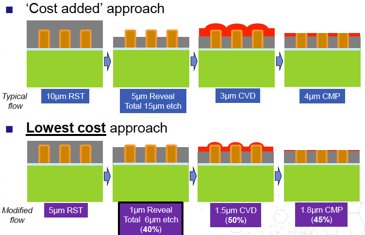
Essentially, a non-controlled approach for the via reveal step requires more material to be left after grind for the reveal etch step. This leftover silicon is called residual silicon thickness (RST), and it affects how thick the chemical vapor deposition (CVD) film needs to be and how long the chemical mechanical planarization (CMP) process takes. The closer you can get to via tips during the grind step, the lower the RST is. End point detection allows for better control over the RST variation across the wafer. “By modifying the approach using in-situ end point detection, we can get closer to the vias in the etch process,” explained Barnett. Figure 1 shows the comparison of a non-controlled process flow vs. a controlled process flow. Only having to etch 6µm of RST instead of 15µm results in a 50% reduction in CVD and a 45% reduction in CMP.
Offering an early look at a breakthrough processes for faster TSV and Cu/SnAg plating chemistries was Bernd Roelfs of Atotech. The company has been working with Fraunhofer IZM-ASSID to optimize plating processes for TSV filling, pillar plating and solder capping.
Roelfs noted that while it would be expected that plating TSVs in interposers should be cheaper than for 3D IC stacks, its actually more costly. When comparing the cost of filling a 5×50µm via for 3D ICs with a 10x 100µm for interposers, it was found that the cost of filling the interposer TSV is 150% higher, due to a disproportionate increase in electrochemical deposition (ECD) plating times. Filling time for the smaller TSV takes 12 minutes, noted Roelfs, while the larger TSV requires 50-60minutes, which dramatically increases the cost. Additionally, the chemical cost is 100% more than it is for 3D ICs due to restricted bath-life of the chemistry, larger via dimensions, more “feed and bleed” and chemical exchange.

The filling height vs. time results from a long initiation time where nothing happens, explained Roelfs. “For the first 2000 seconds, there is no fill. Then, the process slows down halfway through,” he said. Is there an alternative? Yes, said Roelfs, and while its not yet in production, it is showing great promise. It’s called negative differential resistance (NDR), and requires no initiation time, starts filling from the beginning, and speeds up throughout the process. The secret is in the sauce. Atotech’s chemistry additives for NDR include one suppressor and no accelerator. He explained that a suppressor could have different resistivity states that don’t block deposition speeds, but block deposition on the surface. Because there is no accelerator, there are no issues with restricted bath life of bleed and feed rate.
“We still have things to work on. NDR is not in production or qualification. We need to learn how to control the fill rate,” he said, adding that there is very good fill performance purity of the Cu deposit, and it’s a much faster process, but there are still a lot of unknowns.
In his presentation focused on Enabling Technologies for 2.5D Interposer Manufacturing, EV Group’s Thorsten Matthias presented some compelling reasons for implementing its polymer via filling process that we reported on last year at IWLPC 2014. Matthias talked about the current process of record (POR) calling for 5×50µm, saying that based on previous cost analysis involving thinning and etching, it was “a reasonable compromise”, but that this assumption might not necessarily be true any more. “It’s not necessary for every device to go to extremely small vias,” he noted. He added that with larger vias, its also not necessary to completely fill the via to achieve required electrical properties, which affects the cost. He described an Annular Cu TSV that achieves the electrical connection by putting down a thin Cu seed layer and then lining and filling the via with polymer (Figure 2). The result is improved thermal stress and reliability. As completely filling a larger TSVs is more costly, this provides a lower cost solution and a compelling reason to use larger vias whenever possible, thereby reducing the need for thin wafer handling.
He also talked about several ways to address cost issues with temporary bond/debond. For example, in the packaging set up for the TSMC’s chip-on-wafer-on supstrate (CoWoS), over-mold is done before the debond step to give mechanical stability to the thin wafer. He suggested that a similar integration scheme could be used, for example, on a 4-layer stack on an active interposer (or logic controller). He also discussed a “bumping last” approach to deal with a thin adhesive layer. “When to bump or which kind of bump used can impact cost,” he explained. “Thin adhesive layer process integration carries a high cost savings potential due to reduced material usage and reduced thickness.”
We hear quite often that the key to reducing the cost of ownership for interposer and 3D IC processes is for it to get into volume manufacturing. It only stands to reason that the more the processes and tools are put through their paces, the more we can determine what processes can be streamlined. While many PORs were established in the early days of 3D, new developments may be making those initial solutions obsolete. And so, the 3D evolution continues. ~ F.v.T.


