
In Jan Vardaman’s recent readiness report card issued at 3D ASIP in December, 3D IC thermal management issues scored and “F” for lack of a solution o the hot-spot problem when stacking memory on logic. And while she gave 3D IC test a “B” for probe card development, it got an incomplete for reliability data. At the end of her presentation, she invited anyone with new solutions to “see her after class” for grade changes. Ever since, I’ve been on the look-out for reports of advancements in these areas and this past week brought news of progress and different approaches to solutions for both 3D IC thermal management and 3D IC test.
According to a blog post by Ann Steffora Mutschler of Semiconductor Engineering, EDA vendors are tackling the thermal management issue, turning to chip-package co-design solutions to address heat and power dissipation issues that come with 2.5D and 3D IC architectures. Mutschler interviewed a number of EDA experts to get their take on designing for thermal management. She reports that Ansys-Apache. Mentor and Cadence are all developing EDA tools to “do the heavy lifting”.
It seems a good approach – how to design the chip, chip stack, package and board architecture to limit hot spots and localizes heat, and integrate thermal vias and additional TSVs to conduct heat, rather than passing along the problem to be solved by thermal interface materials, heatsinks, and the like at the system level.
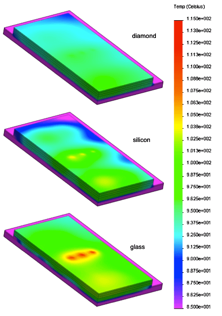
sp3 Diamond Technologies is taking a different path, looking to innovative interposer materials to solve the thermal issues. A feature story in the January/Febuary 2014 issue of Chip Scale Review Magazine, authors Mario Pelella, Jerry Zimmer, and Thomas Tarter, talk about using diamond as the ultimate temperature control material for 3D ICs because of its superior thermal conductivity when compare to both silicon and glass. sp3 has developed a CVD diamond film process that is showing favorable results in temperature dissipation. The article presents details of thermal modeling analysis, as well as a number of ways CVD diamond films can be implemented. Many think diamond as a thermal conductor is cost prohibitive, and the authors would agree in the case of using a solid diamond interposer with Cu vias. They recommend diamond/Cu/diamond interposer that leverages the advantages of diamond at a much lower cost. It’s an interesting read, to say the least, and is worth investigating further as a thermal management solution for 3D ICs.
Also in the Jan/February issue of Chip Scale Review Magazine, Ken Smith of Cascade Microtech, and Erik-Jan Marinissen of imec, report on the success the two organizations have had with probing 25µm diameter micro-bumps on a JEDEC Wide I/O complaint test wafer. This is great news, as testing fine-pitch micro-bumps has been a significant challenge to overcome. The article details the test methodology uses, as well as the requirements specific to probing 3D SICs. While many in the industry continue to question whether it makes sense to perform pre-bond or partial stack tests, and whether its better to just take the yield hit, its clear from this article that the ability to direct probe the micro-bumps offers a cost advantage over the current workaround of creating dedicated test pads, which eat up real estate and add costs, and don’t prove the functionality of the micro-bumps.

Also critical to test is a solid test infrastructure that will provide an effective sequence to test die before and during stacking, and after packaging. Pawan Fangaria recently reported Mentor Graphic’s capabilities in this space in a post on SemiWiki titled Smart Strategies for Efficient Testing of 3D-ICs. Fangaria writes, “Mentor has developed an excellent plug-and-play test infrastructure based on proven standard JTAG (IEEE 1149.1) TAP (Test Access Port) as interface for all dies and IJTAG (IEEE P1687) to model the TAP, test access network, and test components within the die. For accessing the whole package from outside, the TAP at the bottommost die is used, although for testing purpose any die can be used.” Fangaria goes on to give a great step-by-step description of how Mentor’s product works. It definitely helped me better understand how design for test (DfT) tools enable testing of 3D IC stacks. ~ F.v.T.
PS: Incidentally, Chip Scale Review’s January/February 2013 is almost completely devoted to 2.5D and 3D technology features. Be sure to download it and give it a good read.