


Wouldn’t it be great to get a text notification that you are almost out of toilet paper at home rather than when it’s well… almost too late? Or how about an intra-nasal sensor that detects the level of acetone in your breath to tell you if you’re accumulating or burning fat? (It kind of makes my new FitBit wearable activity monitor seem archaic already.) But this is the beginning of the Internet of Things (IoT) and part of the future envisioned by Siemens, Infineon and Fraunhofer EMFT; and enabled by the consortium of the European project Best-Reliable Ambient Intelligent Nanosensor Systems (e-BRAINS, ICT 257488)
While the rest of the world anticipates the coming of 3D ICs using TSVs in high volume manufacturing, Fraunhofer EMFT and its industrial partners, Infineon and Siemens, are more concerned in applying the processes today, in real products that help improve quality of life. My visit last month to Fraunhofer EMFT in Munich gave me a first-hand look at what’s going on at this research institute that, according to program director Peter Ramm, has been working on 3D integration for the better part of 25 years. I talked about some of the work being done through e-BRAINS briefly in an earlier post. Here we dive more into the details around the work specific to Fraunhofer EMFT.
First of all, Fraunhofer EMFT is not to be confused with Fraunhofer IZM-ASSID, which is focused on all silicon systems integration on 300 mm wafers, targeting memory and logic for consumer mobile applications. EMFT is focused on 3D system integration, which may or may not involve Through Silicon Vias (TSVs) and may or may not require interposers. All work is done at 200mm. The TSV line is a 200mm line – vs. the 300mm line at IZM ASSID in Dresden. Ramm explained the reason for this is that EMFT’s industrial partners are also working in 200mm lines. Many of the technologies they are looking to integrate are also being manufactured at 200mm (ie: MEMS devices). According to Ramm, EMFT and IZM-ASSID work together, for example when EMFT has a need for transferring its technology to 300mm.
Beyond industrial partners Siemens and Infineon, the e-BRAINS consortium also includes such research partners as IMEC (Belgium), SINTEF (Norway), Tyndall (Ireland) and CEA (France), as well as a host of European universities, and key industrial partners, as Intel Mobil Communications and SORIN (France). All have worked to develop technology platforms and applications specific to e-BRAINS.
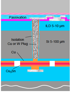
Ramm described some of EMFT’s contributions to the cause that were the outcome of e-CUBES, the predecessor to e-BRAINS that focused on technology development for heterogeneous 3D integration. These include namely thin chip integration, developed in close cooperation with IMEC, and heterogeneous integration by TSV-SLID (solid-liquid inter-diffusion) technology, which involves processes specific to the fabrication of a tungsten or Cu filled TSV on the top substrate, via opening and metallization, thinning, opening plugs, through mask electroplating, and chip-to-wafer alignment and bonding (Figure 1).
The main driver of this work going forward, explained Ramm, is sensor integration, also known as The Internet of Things (IoT). “Interposer for memory is not our focus” he noted. It’s always about 3D integration of a transceiver and a microprocessor to establish wireless capabilities – a critical element for the IoT. Originally, it was thought to be a niche market in Europe and the US. But the onslaught of sensors required to really build a global IoT is expected to change that. He says target applications are not as cost sensitive as consumer applications, and that it’s more about functionality, performance, and miniaturization. Above all reliability is the name of the game.
On the topic of interposers vs. 3D ICs, Ramm says the addition of an interposer will always be more expensive because you are adding a piece of silicon with a redistribution layer (RDL). “While I am convinced that 3D IC integration is the right solution for high-performance applications, we also consider smart interposer technology,” he said.
However, if interposers are used, he advocates thick interposers that don’t have handling issues. He explained that Siemens in cooperation with Fraunhofer EMFT Munich is also developing a high-performance interposer technology, but for thick – and thus stable – interposers. The applied TSV technology – invented by Siemens – is based on photo-assisted etching and a special liquid metal fill process. With that, you can reach TSV diameters in the range of down to 2µm through Si wafers with standard thickness, realizing stable interposers with a low pitch. He also believes in Si interposers over organic interposers because “sometimes you need the more expensive option to ensure reliability.” he said.

Ramm explained that Fraunhofer EMFT’s key target within e-BRAINS is not to invent new technologies, but to apply existing best-suitable 3D technologies and to look at the robustness and reliability of 3D integrated systems. To this end, the consortium has established a number of “work packages” for heterogeneous systems. For example, one focuses on nano-sensor devices and technology. Another, managed by Prof. Maximillian Fleischer, Sr. principal expert research scientist, Siemens, is targeting heterogeneous sensor integration (HSI), establishing roadmaps and building demonstrators for high-level applications to deliver high performance with the appropriate form factor and costs (think: 50 euro application.)
An example of one of five demonstrators that have been built as part of e-BRAINS is a wireless Smart Gas Sensor System that measures the level of C02 of air in the room where optical gas detection is used with photonic structures based on vertical nano wires. One use for this technology is energy efficient building ventilation that might cut energy consumption by one third. Additionally, in the homes of elderly, this can be used to monitor their activity, which is always correlated with CO2 fluctuations home, explained Fleischer. This could be a less intrusive way to safeguard the elderly that imposes less on their privacy than wearable tracking devices.
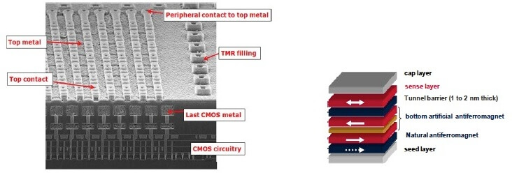
Infineon´s e-BRAINS application demonstrator is the Smart Biosensor Grain (based on Tunnel MagnetoResistance (TMR)), which integrates a biosensor chip with and ASIC, an RF ASIC, and an antennae in a 3D system (Figure 2).
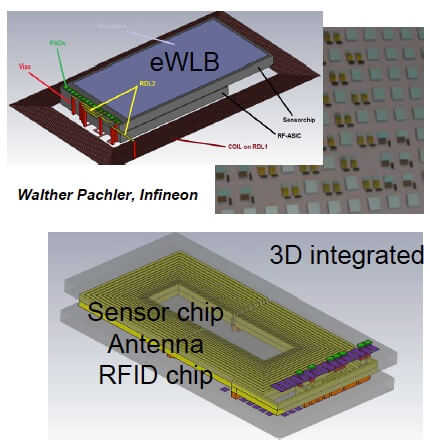 The first version of the Smart Biosensor Grain was based on Infineon’s embedded wafer level ball grid array (eWLB) technology in which the sensor and the RFID were stacked back-to-back, using Cu interconnects in the polymer. Now in development, says Ramm, is a concept for 3D IC integration, replacing the eWLB using TSV SLID that combines 2 ASICS with the biosensor and the antenna. The SLID intermetallic compound structures serve as interconnect as well as for the the antenna fabrication – in one step. “It’s an elegant solution that works,” says Ramm. A paper on this technology will be presented at ECTC 2014 in June in Orlando.
It was clear from my visit that at Fraunhofer EMFT, Infineon and Siemens, 3D systems integration is a reality. As the Internet of Things continues to grow, these seemingly niche applications will increase in volumes, and ultimately pave the way for 3D integration in mobile applications. ~ F.v.T.


