


The 2013 European 3D TSV Summit (January 20-22, Grenoble, France) kicked off with a pre-conference symposium on 3D TSVs for MEMS applications. My initial thought after attending, was that I’m not sure the MEMS people realize this, but some of us who don’t work in the MEMS market but DO work in the 2.5D and 3D IC space aren’t fully aware of the differences between TSVs for MEMS and TSVs for 3DICs (I’m saying this, because based on some discussions following the symposium, I wasn’t the only one with questions.)
I gained some insight thanks to the presentations delivered by Marco Ferrara, MEMS Technology Manager, ST Microelectronics, and Chistophe Zinck, Application Engineering Manager ASE, as well as the panel discussion featuring Ferrara; Tomas Bauer, VP Sales and Business Development, Silex Microsystems; Stephane Renard, CTO and co-founder, Tronics; Iain Rutherford, MEMS Product Marketing & Business line Manager, X-FAB Marco Ferrera, MEMS Technology Manager, STMicroelectronics and moderated by Jean-Christophe Eloy, of Yole Developpment.

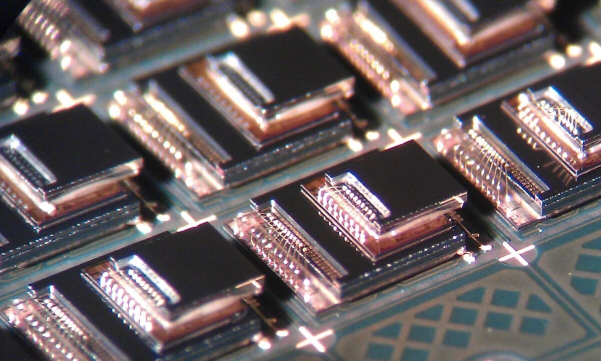
Ferrara talked about ST Microelectronics’ MEMS products, and the via-last and via-first approaches used to build and interconnect them to ASICs. As I understand it, the TSV THELMA/Smeraldo Technlogy via-last approach (pictured above) is a low-cost solution that takes advantage of both front-end and back-end processes, with the main purpose of die size reduction. It allows for the front side of the die to be used entirely for I/O and moves the interconnect pads around to the backside of the die. The MEMS device is then interconnected to the ASIC using traditional wire bond technology. The purpose of the TSV (which is polysilicon filled) is to transfer the electrical connection from the I/Os to the pads. This technology has been in volume production at ST Micro since 2012.
More recently, explained Ferrara, ST Micro has introduced its technology to enable 3D integration of Motion MEMS. This via-first approach relies on polysilicon vias (filled in the front end) and the interconnect is formed using an under bump metallization (UBM) and gold stud bumps, and is assembled using chip-to-chip (C2C) interconnect. ST Microelectronics is fully integrated from design through packaging and test, and Ferrara says they have invested in both via last and via first approaches to provided flexibility, as both will be needed going forward.
Zinck shed some light on the “highly fragmented” MEMS and sensor packaging market. “MEMS are driven by the mobile market, and every application has different requirements for packaging,” he explained, saying the next big move will be system integration which involves a complex architecture, small sizes with multiple functions, which will be “a nightmare for assembly and test subcontractors because they always have to customize something.” To achieve high volumes at low cost he says will require a certain amount of standardization that can only be achieved by standardizing at the wafer level. The key to the success of MEMS proliferation is to understand the delicate balance between performance and cost, Zinck noted. He talked about ASE’s capabilities in MEMS assembly, packaging and test, which includes full WLP MEMS processes (TSV-last manufacturing, wafer bonding, C2W die attach, RDL and bumping.)
The panelists concurred about the importance of TSV adoption in MEMS, driven mainly by form factor advantages. The major driver is with MEMS sensors that interact with the physical environment. It’s more convenient to not have bond wires on the facing side. Rutherford said that TSVs are not a solution for every customer’s needs. “It’s not going to make or break all the business that’s out there,” he said. Some applications are more suited to monolithic integration of MEMS and CMOS circuitry, but they will become increasingly important.
Bauer talked about one of the earliest successful via-first commercial implementations for MEMS microphones Silex (a pure-play MEMS foundry) sold to Nokia in 2006. He said that currently, 50% of Silex’s worldwide customer base is already using TSVs. Rutherford cited medical applications and wearable electronics as examples where device size is essential.
Regarding the cost of TSVs in MEMS – while you pay more for TSVs, there is a trade-off in size reduction that helps cover that cost.
As TSV adoption in MEMS grows, what can the 3D IC market learn from them? First we need to understand the differences between TSVs intended for MEMS applications and those intended for 3D ICs.
First is the size and number of TSVs on the devices. MEMS tend to be larger diameter vias, filled with polysilicon rather than tungsten or copper because they don’t require the same level of conductivity. Additionally, the MEMS wafers are thicker than those intended for 3D IC stacks. “People have been trying for 50 years to make metalized vias,” noted Bauer. “The reliability issue really needs to be taken seriously.”

Renard noted that in MEMS, TSVs are used for protection (MEMS capping) and as an interconnect structure. “When you use TSVs you’re not adding more processes, your replacing processes with others. Therefore the impact on price is not so high in MEMS,” he noted. “There will be economic benefits for sure.”
Eloy put the question to the equipment suppliers and manufacturers in the audience, to get their perspective on the differences between TSVs for MEMS and 3D ICs. David Butler, SPTS, says there’s more mention of “via-first” in 3D ICS as applied to logic and memory and less of “via-last” — with the exception of CMOS Image Sensors (CIS). While from an equipment perspective the fundamentals are the same, production of TSVs for 3D ICS is slowed by other issues, not processes. In MEMS you’re not dealing with high I/Os, aspect ratios are different, and warpage is not an issue.
Glyn Reynolds, of Oerlikon Systems took it a step further to point out differences between TSVs for interposer and 3D ICs. “There are certainly more issued for 3D IC than for 2.5D interposers,” he said. “In 3D IC you need to be aware of the transistors and the keep-out-zone (KOZ).” He says this is the driving force to shrink the TSV size. We need significantly higher aspect ratios for memory and logic (via middle) before backend metallization. And we’re essentially drilling blind holes and filling them with copper, he explained.
Martin Schrems, ams AG chimed in with the voice of experience. He said ams was driven into TSVs early on for a design and process ASIC and discovered the merits of it. “It’s a nice way to standardize electrical connection from the front to the backside,” he noted. “We cooperate with back-end houses. I believe different models will exist, depending on the core competency of each company involved.”
“What MEMS can do for the IC industry is provide decades of experience,” noted Bauer. “We’ve developed a full wafer thickness metal via and we’re excited to find collaboration to serve the IC space.”
Whether we’re talking about MEMS, 2.5D interposers or 3DICs, its clear that TSVs provide a strong process model for lots of devices. There’s lots of energy behind it and the future should prove to be interesting. ~ F.v.T.


