


The way I see it, it was only a matter of time before Nordson DAGE brought its X-ray technology into the 2.5D and 3D IC space. The company has long been the leader for X-ray inspection in the electronics market and is now positioned to address the growing need for wafer metrology and defect review in features such as through silicon vias (TSVs).
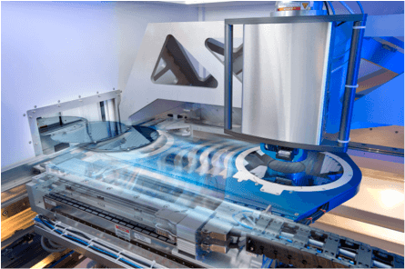
 According to John Tingay, Technical Director Nordson DAGE, this is because unlike other X-ray equipment manufacturers, Nordson DAGE focuses only on X-ray technology for electronics, and not medical or industrial applications. The company is very technology-driven and has been tracking the development of the 3D market since it first emerged, recognizing that X-ray technology will be needed as part of the overall manufacturing capability. This week, the company announces a new tool platform, the XM8000 Wafer X-ray Metrology Platform, not for the purposes of bare wafer inspection, but for automated X-ray metrology and analysis of voids, hidden features and critical dimensions for review and analysis of wafer bumps, TSVs, 2.5D and 3D packages, and MEMS.
With the advent of wafer level packages (WLP) and wafer bumping technologies, followed by TSV processes, Nordson DAGE’s customers have increasingly been using the company’s existing products to detect defects, voids and hidden features in wafer bumps and TSVs, particularly as the entire industry moves to smaller feature sizes, expained TIngay. With the XM8000, Nordson DAGE has taken it a step further, developing a platform that speeds up and automates the process so that the whole wafer can be scanned at high resolution creating a comprehensive hierarchical database of key feature information.
 Tingay explained that what sets Nordson DAGE apart from other X-ray tool companies is its technology. Identifying a gap in the electronics inspection – notably in PCBA – market back in 2000, the company decided to invest heavily in R&D to bring X-ray technology to the leading edge, he explained. Rather than developing either an open or closed tube system, they developed what is known as a sealed-transmissive tube that has the benefits of both the open and closed tube systems without their related downsides, and which resulted in higher resolution, and a brighter X-ray light for improved detection speeds. Up until now, Tingay said the resolution capability of its technology has actually exceeded industry needs. Ironically, analyzing PCB X-ray images is more difficult due to the density and overlapping of the materials and components. In the semiconductor environment the sample is more predictable – you know what should be there, so finding the structure and measuring it is easer, he said.
Beyond the technology, Nordson DAGE also differentiates itself from the competition in that it is vertically integrated. “We build everything from scratch, including our own tube, our own detector design, and our own software. We own the whole technology food chain, which is unique,” explained Philip Moyse, Program Manager, Nordson DAGE.
 As mentioned in a previous post about my visit to Nordson DAGE, the market driver for the development of the XM8000 came from customers who were using the Diamond X-ray inspection system for wafer applications, exploiting the tool’s ability to see small and ever decreasing feature sizes. Moyse said that external data and research validated this market opportunity; forecasting that growth in 2.5D/3D and conventional flip-chip was driving a need for a credible high throughput x-ray metrology solution.
Moyse explained that the new platform required a lot more than just adding an automated handler to the Diamond. In addition to fully automated wafer handling, customers wanted very high throughput, alignment data allowing the results be shown by TSV/bump/die/wafer. And it needed to be fully integrated into the manufacturing process. “Talking to customers, it was apparent that there was initial disbelief that a machine could offer this level of throughput and positional accuracy.” noted Moyse. But they’ve done it.
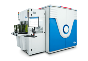
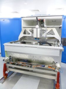
Nordson DAGE’s response to these requirements is the XM8000 fully-automated X-ray metrology platform. Moyse says it achieved fast, (20x faster than the Diamond) high-throughput with real-time analysis that provides both high quality measurements and data. It is clean room compliant and meets the industry standard for handling wafers up to 300mm. Additionally there is a strip-handling version in development. With 450mm not far off in the future, I inquired about that. “Bring it on!” said David Bernard, Business Manager, Automated X-ray Systems, adding that they could be ready for 450mm as early as 2015. For Nordson DAGE, he explained that going to 450mm is merely a handler and chuck size issue; the internal platform remains the same.
Meeting all these customer requirements required a different platform architecture and a calibration wafer to show the capability and provide traceable calibration of the various configurations, measurements and capabilities of the tool, explained Moyse. The sealed-transmissive X-ray tube sits above the wafer sample, and the detector is below. This allows the sample to be brought closer to the X-ray tube and therefore provide the maximum available magnification when required. There are no moving parts above the wafer. Linear motors are on the X-Y axis for precision and maximum throughput. It is fully compliant with the front-end fab environment. Depending on the application, there is either a wafer handler or conveyor system.
So what do all these advanced technology bells and whistles mean for its target applications? Moyse provided the following details:
Wafer bump metrology and defect analysis
As previously mentioned, this tool does not only provide images. It also provides valuable process control data measurements. When configured for wafer bump applications, the machine can indicate:

- The presence or absence of every bump on every die
- The position/position variation of every bump on every die
- The number and size of every void on every bump
- Key features such as diameter and shape of every bump on every die
Additionally, it allows for user definable pass/fail criteria for every measurement. The final data can be processed to give you the results, by bump, die or wafer.
TSV metrology and defect analysis
When configured for TSVs, the tool can do all of the above, but the information the machine holds includes:
- The presence/absence of every TSV on every die
- The length and profile of every TSV on every die
- The number and size of every void in every TSV
2.5D/3D integration: development of overlay measurement
This platform can also be configured to perform overlay measurement of die-to-die or die-to-interposer offsets. Tingay explained this is done using a strip handler versus a wafer handler and as it looks right through the package and sees all levels with high resolution, it does not require a double-sided microscope approach that might currently be used. The system uses fiducials or existing structures such as TSVs, Cu pillars, bumps, and traces to check the overlay.
Bernard explained that as 2.5D and 3D processes become more mature, there won’t be a need, or the time, to do 100% inspection. So, Nordson DAGE is offering customer options for intelligently scanning wafers/die using interactive recipes that will parse or extend measurement points depending on the real time analysis of the results. Metrology and analysis data is provided in wafer map form. “Customers can build a comprehensive database of critical wafer bump and TSV data of every die. Just pick one TSV and have all the statistics,” he noted.
“The platform is capable to perform all of these processes,” noted Moyse. “Ideally customers will be using multiple machines at different places in the fab, each configured to a specific process.”
The new tool’s tagline is “Measuring the Invisible”, which neatly captures its ability to see features and defects, such as voids, that would indeed be invisible to alternative inspection technologies such as AOI or infra-red. “Customers called for this over a year ago, and we’ve been working with our target customer base to test their wafers. Interest is definitely high,” says Bernard.
Because the company philosophy is to manufacture to forecast, rather than to order. Bernard reports that there are final prototypes up and running, and the production pipeline at the company’s manufacturing facility in Aylesbury, UK is already being filled for customer-ready tools. ~ F.v.T.


