
If you’ve followed me thus far in the three preceding posts, well done! We started by questioning the cost assumptions. Then we set the scene to be able to explain the vanishing string current problem, and then introduced the concept of pass disturb.
In this post, as promised in the previous one, I want to deal with pass disturb in more detail, which is one of the more important reliability challenges that these vertical channel 3D NAND approaches have to deal with.
The analogy used by me so far has been a drawbridge that gradually changes from being closed to being open after being cycled through several openings and closures.
In a NAND string where one cell is being read, all other cells must be put into a conducting state. Otherwise we can’t read the chosen cell. Being put into a conducting state requires a relatively high voltage to be placed on these passing cells’ gates. This is unique to NAND strings.
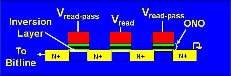
To understand this, let’s take a look at how a cell is read within a NAND string of cells. Figure 1 shows three cells in a NAND string where the middle one is being read. The cells in this case are charge trap devices consisting of a silicon nitride layer sandwiched between two silicon dioxide layers.
To be able to read the middle cell, we need to apply a low voltage (Vread) on the gate of that cell where the magnitude of this voltage is between the programmed and erased threshold voltages of these devices.
To be able to electrically connect this cell to both ends of its NAND string, all other cells in the string must conduct (that “inversion” channel in this case, (but for the sticklers among you, it can be an “accumulation” layer too).
To make this connection, the read-pass voltage (Vread-pass) has to be higher than the highest programmed voltage. Otherwise, there’s a good chance that these cells won’t electrically connect to the cell being read.
Applying this high voltage to an erased state charge trap cell causes the problem. This is the drawbridge that gradually opens up after repeated openings and closures. We get these passing cells gradually being programmed after multiple read operations.
Samsung admitted in 2006 that “the use of thin tunnel oxide is a road-block for the SONOS device to come into high-density NAND flash memory.” SONOS is the name given to the charge trap flash (CTF) approach that is now being touted by Samsung and Toshiba (and others) as the way to do 3-D NAND. The tunnel oxide is the insulator through which electric charge is placed and removed from the silicon nitride layer (“N” in SONOS).
This admission apparently took them three years to realize since their first paper in 2003 used a thin tunnel oxide layer. The road-block standing in the way is pass disturb.
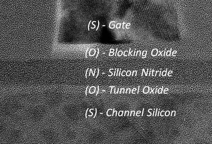
Let’s have a look at what the SONOS structure really looks like. Figure 2 shows an extremely high magnification cross section of a thin-film transistor (TFT) SONOS device that my company made.
The tunnel oxide is so-called because it is the path through which charge passes by way of quantum mechanical tunneling. This charge gets trapped on the nitride layer and causes the nonvolatile memory effect of changing the device’s threshold voltage.

When SONOS is used in a non-NAND approach (in other words, with thin tunnel oxide), some very attractive characteristics are achievable. Such cells have been successfully programmed and erased for one hundred million cycles at around 12 V. The key is the use of a thin tunnel oxide.
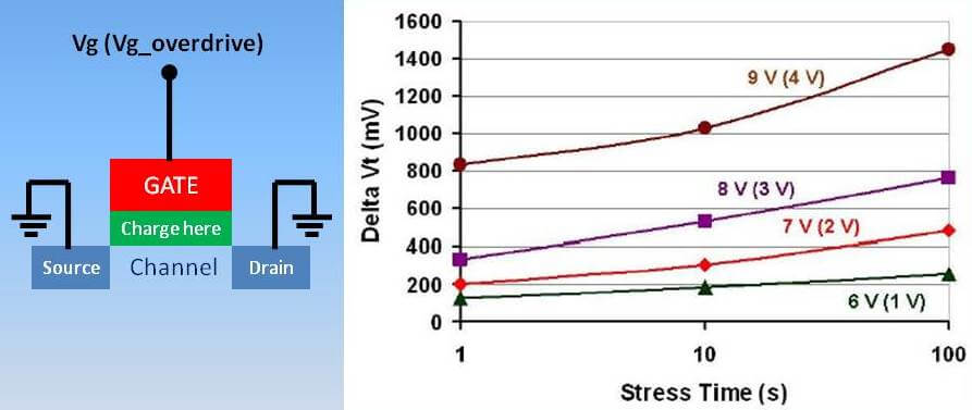
But as Samsung noted, such thin tunnel oxide SONOS cannot be used in a NAND string, whether it be in 2-D or 3-D. The reason can be seen from figure 3 where the threshold voltage shift (Delta Vt) is measured of a passing cell within a NAND string when various read-pass voltages are applied. Any shift like this is unacceptable.
What they did to mitigate (but not eradicate) this effect was to thicken up the tunnel oxide. This caused a cascade of necessary changes to the basic SONOS structure and resulted in their TANOS approach. The “ANO” supplants the “ONO” and stands for aluminum oxide as the blocking oxide, silicon nitride as the charge-holding reservoir (as before) and a tunneling oxide much thicker than SONOS. The “T” stands for tantalum nitride and is also needed to avoid charge injection from the gate during erase.
Major consequences of these changes are: limited program/erase (P/E) cycling endurance (a few thousand times due to damage evolution in the thicker tunnel oxide); much higher P/E voltages (now at or above 20 V); thicker dielectric (ANO) stack. The latter is troublesome for the 3D vertical channel NAND approaches since twice this thickness is in both pitches of the cell.
A very interesting fundamental interaction is the one between the worst-case string current and the read-pass disturb. Remember in the previous post how we could dramatically increase this current by increasing the read-pass voltage? And remember how important this is when we have a disordered channel? Well, now you can see how constrained we are in doing this precisely by disturbs. And this applies even to the thick ANO stacks.
This is most probably part of those “ongoing challenges” reported recently with vertical channel 3D NAND.
Wouldn’t it be nice to get rid of these pass disturbs completely AND maximize the worst case string current AND use thin tunnel oxide SONOS with all its advantages? And all at lower cost than these vertical channel 3-D NAND approaches? More on how some other time. ~ A.W.