


2.5D interposers sparked a good amount of discussion at this year’s 3D ASIP conference (December 11-13, 2013, Burlingame CA), with a session devoted to “Interposers for all of Us” and other presentations scattered throughout the program to address such issues as thin wafer handling, and heterogeneous integration.
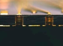
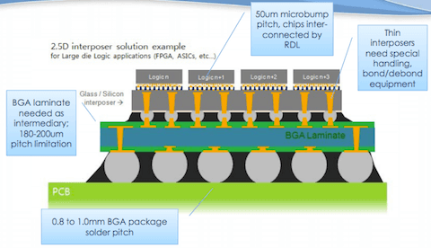
Weighing in on Si interposer innovations was Peter Himes, of Silex, who talked about how Silex has leveraged TSV technologies from MEMS wafer fabrication to create what he calls “Interposers for the Common Man”. In his presentation, Himes paints a picture of the current “interposer dilemma” that begins with the challenge of creating a package with small, densely packed interconnects with an overall package height under 400µm. The current approach uses ultra-thin wafers that are then mounted on an organic package substrate as the interposer handle. Himes says the result is a solution that adds cost and complexity back into the package in a time where the industry is looking for affordable, straight forward solutions (Figure 1).
Himes described Silex’s all-silicon solution that eliminates the need for a package substrate, but interconnects directly to the printed circuit board. The interposer is a full thickness wafer that doesn’t require thin wafer handling or an organic substrate. “By using a full thickness wafer, we’re putting TSVs in something that can stand on its own and doesn’t need an organic substrate or thin wafer handling,” explained Himes. “You also eliminate a whole set of thermal components due to CTE mismatch.” Additionally, a Si substrate can be functionalized with passive and active elements (Figure 2).
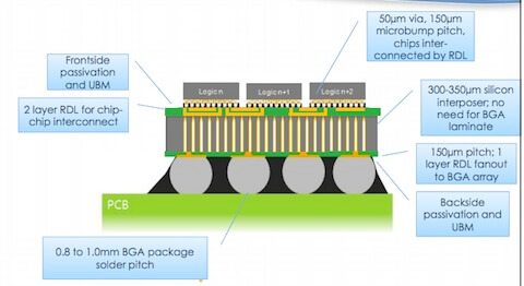
Silex first developed its Sil-Via rigid interposer in 2005, and implemented it in a MEMS microphone in 2006. Its been in volume production for MEMS applications for over 7 years. The challenge of adapting for the needs of 2.5D interposers, says Himes, was creating higher aspect ratio vias at higher density than is typical for MEMS applications. In 2012 the company has demonstrated a 2.5D interposer with high density RDL and low density through silicon vias (TSVs) – 50µm vias with 150µm pitch. Himes explained that via density and pitch is driven by BGA density on the bottom, not the I/O density of the chip. The RDL process is also adapted from MEMS applications, and uses a similar polymer RDL as was described by IME. Essentially, a high-density RDL needs low-density TSVs and can support the BGA fan-out TSV density.
Cost of Si interposers is another issue Himes says can be addressed with the rigid interposer technology he described. The company has done a cost analysis that shows although Si is more expensive; with this approach you eliminate a layer and assembly costs. The company is currently working with Broadpac on test chips, performing thermal cycling tests to prove the reliability of the solutions.
From the organic interposer camp, Javier DeLaCruz, presented an “Industry First” from eSilicon; a very large (50mm x 50mm) organic interposer (larger than a Si reticle) that he says opens up options for 2.5D heterogeneous integration, and is a lower cost, easier to handle interposer solution than Si for certain applications. The interposer targets networking and super computing. “A cell phone is the wrong place to be looking for this. It’s the size of package you’d expect to see in networking,” explained DeLaCruz, “2.5D device size is dictated by the size of the silicon on top. It doesn’t need to be a small package. With organic, you don’t have to pay as big as a price for a big area.” (He showed us an impressive photo, but unfortunately it’s not available for public release. Thus, the benefit of attending the conference!)
DelaCruz used this product introduction to highlight the overarching need for a new approach to system architecture. He said the focus has been on the foundry and assembly house readiness, when we should really be looking at what needs to be done differently in physical design and design for test (DfT). “We need to extract all the advantages from a technology and consider things completely differently,” he said. “It has to start at the architecture phase, what are we going to make? Don’t consider past limitations and start fresh.” Ultimately, we need to think of the entire system in one shot (can you say “Interconnectology?”).

“Don’t focus on the smallest node available, focus on the most ideal node for each of the technologies you need,” explained DeLaCruz. “That way you can increase performance without taking the hit of the higher NRE.” Die needs to be designed specifically for 2.5D and 3D. He explained how this puts packaging engineers in a unique position of having to react to system architects. “They’re going to work in a world with constraints that cease to exist,” he noted.
2.5D heterogeneous integration is a different game with different rules, explained DeLaCruz. “If you bring in all your memory connections into a package, all you have going out is control pins and high speed SERDES, which affects the layer count and body size of the package,” He said. “A PCB that normally has 36 layers now has six. The PCB and contract manufacturers get less revenue, because the value is now in the package.” In 2.5D heterogeneous integration, the package size is gated by silicon arrangement rather than ball count, and will have a lot of power delivery. Additionally, test-pin requirements need to be considered to keep test time low.
While the industry continues to debate between Si, glass and organic as the interposer material, DeLaCruz puts his two cents in in favor of organic interposers: an organic interposer routed as densely as silicon is an enabler, he explained. There is no silicon size limitation, you don’t have the same stepper costs, and you can put a lot more into a 2.5D structure. The infrastructure is coming up to speed, and it will be there. From an assembly standpoint, as long as you account for CTE mismatch, its easier.
“I’m not saying Si Interposers don’t have a place, but on large, high-end networking it’s not the best solution.” says DeLaCruz. “Pushing limits on silicon size isn’t the way to do it. The way to do it is to jump to the next technology. We’re talking about higher performance at lower cost. It’s not a matter of will it happen, it’s a matter of when it will happen. We’re on a path we can’t turn back from.” ~ F.v.T.


