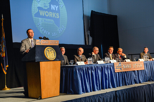
Word on the street is, New York will soon be known as Nano York, with all the money the state is pouring into nanotechnology research and development. The most recent announcement by Governor Cuomo is a $1.5 Billion Public-Private investment intended to turn the Mohawk Valley (Utica) into the next major hub for nanotechnology research.
A consortium of global technology companies headquartered at the CNSE-SUNYIT Computer Chip Commercialization Center will be lead by Advanced Nanotechnology Solutions Incorporated (ANSI), SEMATECH, Atotech, and SEMATECH and CNSE partner companies, including IBM, Lam Research and Tokyo Electron. The consortium will focus on R&D for computer chip packaging and lithography development and commercialization, and will reportedly drive a host of new technologies and products in the consumer and business marketplace, including smart phones, tablets, and laptops; 3D systems for gaming; ultrafast and secure computer servers and IT systems; and sensor technology for emerging health care, clean energy and environmental applications.
*******
Known Good Die (KGD) is a recurring theme in this industry, and is said to be the reason why multi-chip modules (MCMs) – the precursor to today’s 3D ICs – never took off. Over the past year, its been suggested that Probably Good Die will be sufficient for 3D stacking. In a recent post on the topic, Semiconductor Engineering’s Jeff Chappell talks to a number of test companies about the challenges of test when TSVs are involved, in particular with 3D IC stacks, and the changes in test strategies under consideration.
While it would seem that 100% KGD is essential, it may not be economical. “In some manufacturing scenarios, particularly among high-yield devices such as memory, it may prove cheaper to depend on a probably good die test strategy, even though it means some yield loss at final packaging, as the cost of that loss would still be less than that of testing for 100% KGD prior to packaging,” writes Chappell.
********
The latest from the monolithic 3D world, research institute imec, has announced a new approach to vertical memory. EETimes journalist Janine Love, posted a great article outlining the details of the work being done to develop alternatives for lithography in building layered flash. According to her post, the key is a better channel material to allow for multi-layer stacking with only one lithography step. To this end, imec has developed a laser annealing process to recrystallizing polycrystalline channel material. “In this technique, a laser is used for very local melting of the polysilicon material, which can make more monocrystalline materials. The melting occurs at the top of the wafer. When the laser is removed, the heat travels down the channel and continues the recrystallization,” writes Love. You can find the full story, 3D Memory Gets a Boost, here.

Not to be outdone, researchers from Taiwan’s National Nano Device Laboratories have fabricated a monolithic sub-50nm 3D chip that integrates high-speed logic and nonvolatile and SRAM memories. According to a post in Solid State Technology, researchers fabricated the device layers by depositing amorphous silicon and crystallized it with laser pulses. The work will be presented in December at the IEEE International Electron Devices Meeting (IEDM) In Washington DC.
******
In an essay posted on EDA Café, Bill Martin, E-System Design President & VP of Engineering, takes a walk down memory lane detailing 4 Generations in the History of Electronics. Each generation was highlighted by a major technology advancement for the times, from vacuum tubes to transistors, silicon, asics and 3D integration. He refers to the 4th generation, the one we are currently in, as the Lost Generation due to the fact that much of it was spent recovering from various economic crises.
My favorite part? He calls 3D silicon and 3D packaging the “glimmer of hope” for the 4th generation. He also addresses one of the ongoing questions about which 3D technology will be the big winner. He writes “Some may state that one 3D technology will win out over the other. I do not believe this. Both technologies have so much to offer in different areas: one in silicon processes, while the other focuses on packaging. Using only one of these restricts the gains if solely based on the chosen technology: the yield is a linear progression. If both technologies are used, however, gains can have multiplying effect.” I couldn’t agree more. If you haven’t had a chance to read this essay, I recommend you do. ~ F.v.T.