


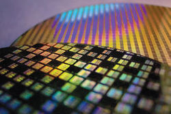
The IEEE 3D Systems Integration Conference (IEEE 3D IC) is a unique event that is a truly international effort in assembling all those involved in research and commercialization of 3D IC and 3D systems from around the world. Location for the event rotates annually from Munich to Tokyo to San Francisco. This year, the event tool place in San Francisco and I was fortunate to attend.
Over the course of 3 days, invited speakers reported on development work in Europe, the US, and Asia, shared manufacturing success stories, and participated in a lively panel discussion focused on both progress and remaining obstacles to 3D IC and 2.5D high volume manufacturing. There was also a host of technical papers and posters to demonstrate that 3D IC is still a very compelling area and worthy of focus.
Motivation for 3D IC
Often lately, we hear that enthusiasm for 3D is waning. The continued delay of commercialization, and little forward movement on such issues as supply chain, liability, and thermal management contributes to that perception. But the motivation for adopting 3D IC technology is as compelling as ever.
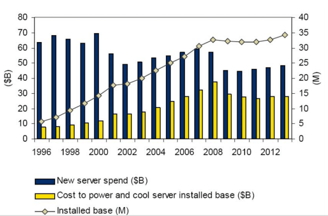
In his tutorial on 3D Design, Paul Franzon, of North Carolina State University, revisited the many reasons why 3D IC is a good idea, particularly noting that current systems are “performance-constrained by power consumption.” One compelling data point Franzon shared was that 2% of worlds power is consumed by servers. Of that, only 30% goes to power the electronics themselves. The remaining 70% is used to power and cool the server base itself.
With regards to conventional CMOS scaling and its impending demise, Franzon noted “We’ve achieved exponential gains without scaling in the past. We can again.” He explained that by combining 3D ICs with emerging computational technologies, we can achieve exponential gains when we lose CMOS scaling at 7nm.
According to Franzon, digital components are easy to scale, analog are not. So a good argument for 3D heterogeneous integration is that it affords us the ability to save design and manufacturing costs by mixing advanced node digital components with legacy node analog in the same device.
On the cost side, because 3D IC processing adds 15%+ to wafer processing costs, and silicon interposers (2.5D) add 25%+ to the cost of packaging before silicon, its important to seek out areas where 2.5D and 3D reduces cost down the line. Franzon pointed to cost advantages of heterogeneous integration, having on high pin count packaging, reduced cooling overhead and yielded silicon cost savings. “As long as the cost of 3D Or 2.5D integration is less than $20.00, than money is saved due to increased yield cost reduction,” he explained, citing Xilinx Virtex 7 as an example.
In his presentation “A Perspective on Manufacturing 2.5/3D”, Tezzaron’s Bob Patti also addressed cost, saying that in the near term, we’ll only be saving money at the system level. “In many cases, that’s good enough,” he said.
3D: Coming of Age
Patti’s opinion is that 3D is coming of age, transitioning from “a neat R&D project” to a real manufacturing technology. “Its not just about the transistor any more,” he noted. “It’s all about the wire and 3D provides a shorter interconnect with through silicon vias.”
3D is rich and has a varied technology span, noted Patti. There’s not going to be just one that solves all the problems. “If we’re going to proliferate this technology, we need the designers and engineers to understand what can be done with it,” said Patti. And contrary to popular belief, there is an ecosystem for 3D ICs. It’s just young, but it is in exponential growth mode, and vendors are “3D aware” he says.
While Tezzaron is primarily a 3D IC memory manufacturer, the company has recognized the benefit of 2.5D, and has been an active participant in the IME Consortium. One lesson learned at Tezzaron through this experience? “We need to deliver more than the point solution for Memory,” said Patti. “We need to deliver system-in-package (SiP) designs.” Patti also remarked that while 2.5D isn’t as good as 3D, it allows you to get 90% of the performance improvements of 3D.
Supply Chain Progress; Remaining Obstacles
One highlight of this event was the panel discussion moderated by Jan Vardaman. The assembled panelists represented world-wide perspective and included Bob Patti, Dimitrios Velenis, imec; Doug Anberg, Ultratech; Dongkai Shangguan, NCAP; and Mitsumasa Koyanagi, Tohoku University. Questions covered all the usual topics including design tools, material and equipment issues, improving cost, interposer materials, and test.
On design tools, Patti said the basic tools are there for simple design. What we’re missing is the next level of automated tools for 3D place and route. Shangguan’s wish list included simulation tools for high frequency performance, design-for-test (DfT) and design-for-manufacture (DFM) tools. “As the process becomes more mature, we will gain knowledge in the transfer process,” he noted.
Koyanagi identified a need for tools for “total design for 3D IC I/O design, and a tool that optimizes power consumption”. Velenis agreed that we need tools to examine the total picture, saying that imec is working on DFM tools to evaluate stress and the impact on transistor functionality.

Regarding materials and equipment issues, Anberg offered the lithography tool perspective, saying that it would be helpful to know from the industry what the overlay requirements are. “What do we need to do to support TSV and interposer applications?” asked Anberg. “We get a significant range of requirements, but it would be nice to have a firmer roadmap on that. There are a lot of unique requirements that would be helpful to understand so we can build a tool that can work.”
Patti said he would like to see progress in HVM metrology and in-line test tools. While there are lots of tools related to this, they are not geared towards high-volume production, he explained. He would like to see equipment and processes that are geared for batch processing vs. unit processing.
Koyanagi said he would like an in-line stepper and a high accuracy mask aligner that can handle a 13 inch mask, which requires larger reticle sizes than currently available. Both he and Shangguan said temporary bonding, debonding, (TB/DB) and thin wafer handling are still lacking in both the equipment and material solutions, and tools and materials that provide a very high bonding and debonding yield are critical. On this topic, Velenis said “We are optimistic that proposed approaches will improve yield and throughput and reduce cost.”
Anberg said Ultratech is looking into increasing reticle field sizes, and expect them to double and triple for certain applications in the next few years. Patti noted that Tezzaron solution with regard to TB/DB is to avoid it all together. “We don’t believe in thin wafer handling”. They use a wafer stacking process (Fa-Stack) that doesn’t require temporary bond/debond or thin wafer handling.
All agreed that the path to reducing cost is through improved yield and throughput. “High volume manufacturing itself would be the biggest improvement in cost,” noted Velenis, adding that reducing complexity of the processes would go a long way to reduce cost.
 On the topic of Si vs. glass vs. organic as the chosen interposer material, it seems Si is still leading the charge. While many think glass is “a happy medium” because it doesn’t have the routing problems organic interposers have, and has a better coefficient of thermal expansion (CTE) mismatch, it is a poor thermal conductor. Organic is half the cost of silicon, but it can’t handle the finer feature sizes. “Silicon interposers will have value because we can put transistors on it and can go to 2µm line and space,” he said.
According to Koyanagi, companies in Japan won’t compete with TSMC for Si interposer business, but they are strong in materials especially glass, and have invested in developing through glass via (TGV) processes. Velenis said the biggest cost benefit of TGV, which is a serial process, is to go to panel vs. wafer production.
Offering his input from the audience, Phil Garrou, pointed out the lack of infrastructure for glass. “Glass isn’t real until it’s coming from the flat panel display industry. It can’t be done at assembly houses. If the flat panel display guys think it’s worth the money, then it will be real,” he said.
Vardaman summed the panel up in a few sentences. There’s improvement in the design side of things. We still have material and equipment issues to iron out. If you can avoid thin wafer handling, do it. Silicon interposers will make it. Cost is the most critical thing and the way to deal with it is through yield improvements. Progress is being made in test. Thermal issues are still the big question mark.
So is enthusiasm waning? Not inside this 3D IC inner sanctum. Here, hope springs eternal. ~ F.v.T.


