


 STMicroelectronics brought a “Who’s Who” of thought leaders from across the MEMS and Sensors ecosystem to Santa Clara, CA, on September 10, 2013 to deliver practical and expert tips to the assembled attendees on using MEMS sensors to optimize performance, size, power consumption, and product cost for consumer and industrial electronic products.
During this Shaping the Future of MEMS and Sensors Summit, top technologists from ST and from the MEMS community demonstrated how they are adopting sensors to enable applications, augment the user experience, and expand markets. Attendees also heard Industry visionaries describe where it is they expect the next-generation of MEMS sensors will be creating opportunities to shape the future of electronics.
Of greater interest from 3D InCites’ perspective, attendees also learned from several of the distinguished speakers, how TSV / 3D IC processes, long part of commercial MEMS fabrication standard process flows, will contribute even more in the future to add value and reduce costs in next-generation MEMS sensors.
![]() Among the highlights from the summit were the talks given by Becky Oh, PNI Sensor Corporation, on the greatest MEMS sensor commercialization stories you probably didn’t already know; Janusz Bryzek, Fairchild Semiconductor, on the journey to a Trillion Sensor future; Benedetto Vigna, STMicroelectronics, everybody’s favorite MEMS executive, on ubiquitous MEMS and Sensors in wearables; and Alissa Fitzgerald, A.M. Fitzgerald & Associates, on the challenges of MEMS Integration into medical solutions (this talk being one of the talks that prominently featured TSV / 3D IC technology).
Among the highlights from the summit were the talks given by Becky Oh, PNI Sensor Corporation, on the greatest MEMS sensor commercialization stories you probably didn’t already know; Janusz Bryzek, Fairchild Semiconductor, on the journey to a Trillion Sensor future; Benedetto Vigna, STMicroelectronics, everybody’s favorite MEMS executive, on ubiquitous MEMS and Sensors in wearables; and Alissa Fitzgerald, A.M. Fitzgerald & Associates, on the challenges of MEMS Integration into medical solutions (this talk being one of the talks that prominently featured TSV / 3D IC technology).
One very interesting comments about the MEMS and Sensors Summit, overheard from a MEMS veteran in a sidebar discussion during a change-over break, was this: “I have never seen this many end-users of MEMS devices at a symposium before. … It seems to me from the questions asked of the speakers that many in attendance are neophytes to the field.”
At 3D InCites, we recently promoted a conversation on the 3D IC supply chain, to wit: “There has been no shortage of industry executive panels focused on the 3D IC supply chain. Additionally, there are continually calls for collaboration to help solve remaining technical challenges and lower cost of ownership to bring 3D IC to market. However, in all of these panels, we don’t hear the answer to the question ‘how?’”
I think the answer to “how” lies, at least partially, in the TSV / 3D IC work already developed and commercialized by the MEMS device and MEMS foundry industry, something which might not yet be well-known to “neophytes to the field” of MEMS technology, regardless of how experienced those MEMS neophytes might be with leading-edge CMOS IC fabrication.
Hoping to further promote the 3D IC supply chain conversation, I spoke at greater length with Alissa Fitzgerald (Founder and Managing Member) A.M. Fitzgerald & Associates; Mike Shillinger (Founder), from the Santa Barbara, CA-based MEMS foundry IMT; and with Peter Himes (Vice President, Marketing & Strategic Alliances), from Silex Microsystems, a MEMS foundry located in Järfälla, Sweden.
It’s been said about TSV / 3D IC that it is one of the few cases where the “PowerPoint Engineering” presentations of the TSV idea are so convincing that it is actually hard to oppose the technology, but that its physical existence outside the slidedeck is somewhat hard to verify.
Unless you look for evidence from within the MEMS industry.
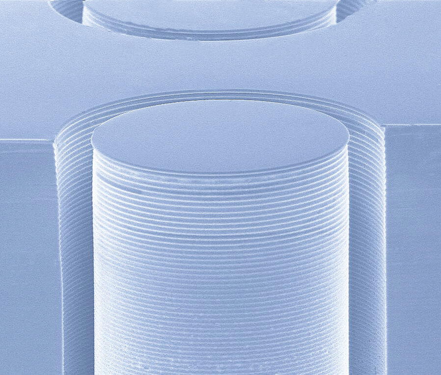
In distinct contrast to the PowerPoint engineering meme, here are proof-in-the-pudding examples of TSV / 3D IC processes used in commercial devices fabricated in the MEMS world: the Avago FBAR MEMS acoustic filter (now more than a billion devices produced per year), and the Epcos MEMS microphone (these examples per Brandon Prior, Prismark Partners, ca. 2010).
And here are more: at Silex, the Sil-Via TSV fabrication process went into production in 2005 for a MEMS microphone application, running as many as 2000 6” wafers per month at that product’s peak. The word now is that half of Silex’ current customers use the Sil-Via TSV design for making electrical connections to MEMS element.

And IMT has been steadily producing RF switches, DC switches, and 2.5D interposers for its customers using TSV technology. AC switches have been in production at IMT from 2003, and RF switches from 2006. That seems real enough to me.
And what about the cost of TSV / 3D IC processes?
Peter Himes, Silex, sees the CMOS IC world looking for the cheapest system solution that gets them to market – if that means 14nm at TSMC that’s great; if it means doing something in the package, or with 2.5D interposers, so be it.
The Xilinx FPGA-on-interposer case makes sense, but so far it’s only them taking the 2.5D leap. Himes thinks the world needs to see costs reach the $10 chip set for consumer applications, rather than the $2000 chip set for enterprise applications, as the price point where interposers achieve lift-off.
Himes says we need to see “the interposer for the rest of us.”
To that end, Silex offers their MEMS-side experience and perspective for 2.5D interposers, and Silex is working now with their partner BroadPak to form an even stronger value proposition for the CMOS IC world; for example, System-on-Chip (SOC) houses that want to marry an ASIC with memory using interposers or 3D IC.
Mike Shillinger, IMT, thinks cost is a chicken or egg discussion. Per his recent conversations at Arizona State University, TSV for CMOS IC is expensive right now, one reason being it’s not yet in volume production at the CMOS fabs. Until production volume goes down, costs will remain high, which means the CMOS IC world will continue to integrate increasingly dense SoC solutions first, for cost reasons, before moving later to TSV / 3D IC.
Alissa Fitzgerald adds that one reason MEMS device fabricators moved from the early MEMS+CMOS-on-one-chip integration — which was a kind of holy grail and was strongly advocated by Analog Device, among others, up until 5 or 6 years ago; to other schemes like MEMS and CMOS integrated in a Multi-Chip Module (MCM), or heterogeneously integrated as 2.5D or 3D IC — is due to the disparity of the photolithography systems used for the two technologies, with feature sizes somewhere at 0.5µm and up for MEMS, whereas today’s advanced CMOS is now working at the 28nm process node.

Different wafer sizes, mostly 150mm and 200mm diameter wafers for MEMS fabrication, and 300mm for CMOS IC fabs, also account for what forced new ways of thinking about MEMS and CMOS integration, and may have been another part of the economic and technological push that resulted in the pronounced use of TSV / 3D IC technology in MEMS today.
How closely then has the CMOS IC world been paying attention to MEMS TSV / 3D IC? What kind of collaboration is happening now between TSV / 3D IC development teams in CMOS IC and their counterparts in MEMS?
![]() With TSV / 3D IC technologies, Fitzgerald says the CMOS IC world is currently seeing the same kind of issues with which MEMS practitioners have long been familiar. In particular, issues related to stress; an example of which is the stress created by small temperature excursions in wafers, or in finished devices, that can cause delamination of some of the thin films out of which the MEMS or CMOS IC products are built.
With TSV / 3D IC technologies, Fitzgerald says the CMOS IC world is currently seeing the same kind of issues with which MEMS practitioners have long been familiar. In particular, issues related to stress; an example of which is the stress created by small temperature excursions in wafers, or in finished devices, that can cause delamination of some of the thin films out of which the MEMS or CMOS IC products are built.
The MEMS world hasn’t completely conquered these issues as yet, but, on this topic, the MEMS design community is clearly ahead. According to Fitzgerald, CMOS IC needs to become more familiar with the design and modeling tools MEMS has now – and that’s why CMOS IC customers have been reaching out to A.M. Fitzgerald & Associates, with its deep roots as a MEMS consultancy, for expert help.
Echoes Shillinger, IMT: “The CMOS chip guys are coming to us for help on via-last processes.”
![]()
Regarding real problems from the point of view of the logistics, cost, and supply chain for TSV / 3D IC technology, Shillinger says the MEMS industry continues to work through those. In IMT’s case, significant time has already been spent on reducing TSV costs by optimizing the (relatively slow) copper electroplating process used for TSV filling. What IMT sees now is that many people from the semiconductor industry are coming to IMT to be schooled on TSV / 3D IC MEMS processing. IMT had an early start with those technologies; now, in 2013, they are mature technologies and there is information and process know-how ripe for the gathering.
Says Himes, Silex, about TSV / 3D IC: “It’s an engineering challenge. We use what we have and we are pragmatic setting up a supply chain solution that’s easy for customers to grab onto. Customers don’t need the Cadillac solution for everything – cost and price points are key.”
“We need more 3D IC guys talking to MEMS people. There’s lots still to learn, and MEMS has already struggled and learned,” says Alissa Fitzgerald, about industry collaboration. “There’s room for improvement and for standardization. Working together on TSVs for optical imager arrays, like bolometers, for example, where you are aiming for the absolute highest fill factor of active area to circuit, would be a great place for the MEMS and the CMOS IC worlds to collaborate.”
Neophytes rejoice.
 And be relieved that perceived problems from the point of view of logistics, cost, and the supply chain for TSV / 3D IC technology have already gone a long way toward being resolved by the MEMS industry, where there is fertile ground for fruitful, rewarding collaboration.
From Petaluma, CA, thanks for reading. ~ PFW


