


I admit, I always have my 3D glasses on at conferences. But even though the title of this week’s MEPTEC event was “The Semiconductor Roadmap Symposium, A Collaborative Update From Standards Bodies, Industry Groups and the Entire Supply Chain”, it could have been “3D TSVs Roadmap Symposium…” based on the direction the panel discussions took throughout the day.
Not that I’m complaining mind you. For me it was a day well spent to hear the opinions of executives from across the industry, and their views on 3D ICs. In fact, when SEMI’s Karen Savala presented her keynote, “The Collaborative Engine: Enabling Innovation in Microelectronics” and spoke about collaboration activity around PV and the transition to 450mm wafers, I found myself wondering, “why is she talking about this at a 3D IC symposium?” and then reminded myself that it wasn’t intended to be.
In addition to the keynote, the day was divided into four panel discussions: Product Drivers, Manufacturing Drivers, Electrical Performance Requirements to Meet Emerging Interconnect Standards, and The Importance of Industry Organization Collaboration. Each panelist had 3-5 (or 10 minutes in some cases) to present their position, followed by a Q&A session. What transpired was lively discussion on all counts. There were also “scribes” assigned to each session to summarize and present the summaries at the end. They were Paul Werbaneth, 3DInCites; Linda Mathew, TechSearch; Scott Jewler, SVXC; and Hongxia Sun, STATSChipPAC. The scribes have agreed to participate in a Round Table Discussion on 3D InCites next week to present these summaries virtually. My goal here is to pinpoint some key takeaways and panelist comments on what continue to be key issues for 3D ICs.
Fun Facts…
Netflix is the #1 driver of traffic on the Internet today. Mudasir Ahmad, Cisco said that 91% of future traffic will be video. Today 50% of all Cisco traffic is video.
A Cisco CRS-3 can download the entire printed collection of the Library of Congress in one second.
On Moore’s Law…
Probably one of the best explanations I’ve ever heard on Moore’s Law came from Karen Savala’s keynote: “Moore’s Law was a historical observation extrapolated to the future. Through collaboration it became an industry-wide agreement for agreed upon improvement over a specified timeframe.”
Ahmad was more concerned with Metcalfe’s Law, which drives the connection of network devices. Every network is measured by the square of the number of devices connected to the system. With the Internet of Things, the network will grow.
Broadcom’s Tom Gregorich, who noted that the industry’s “chief engine” is slowing down, asked rhetorically, “Are there alternative technologies to supplement the benefits of Moore’s Law? There probably are! We just never looked because Moore’s Law is so strong.” He also said there’s no “silver bullet” solution and filling the gaps left by Moore’s Law slowing will be incremental. And lastly, “Mixed signal and 2nd tier suppliers can be studied to understand how to survive without depending on Moore’s Law for improvement.”
From Abe Yee, nVidia: GPUs will continue on Moore’s Law and double performance every two years.
On the need for 2.5D and 3D ICs…
The award for the most provocative statement on this topic goes to Cisco’s Mudasir Ahmad who said, “For us, the end game is not TSVs and 3D ICs. Our end game is Silicon Photonics. The benefits are huge, the trouble is we can’t get there without going through the others (2.5D and 3DCI).”
Yee noted that “memory is the gas that drives the GPU engine.” High bandwidth memory required to break the memory wall requires 3D TSVs. Connecting that memory to the GPU requires 2.5D with TSVs.
“We’re there. We’ve been there,” said Ahmad, but added that Cisco continues to push monolithic; “ We’re kicking the can down the road… waiting to see if there’s an easy in-between solution without having to deal with big investment and architectural shift.”
Predictions of 2.5D and 3D TSV adoption…
Richard Crisp, Invensas, offered probably the most sobering but honest response. “The industry is always looking for the cheaper way to do things. The industry embraces evolutionary rather than revolutionary change.” He added that there’s even the inclination to sacrifice performance for lower cost. My response to this? Sad but true.

Tom Gregorich noted, “Successful 3D TSV products must be preceded by successful 3D products using other 3D technologies.”
In nVidia’s world, “2.5D and 3D will be required and I think it’s just around the corner,” Yee said.
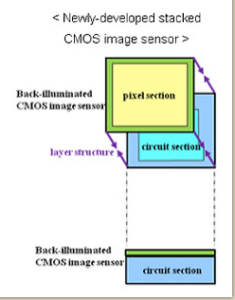
In the world of CMOS image sensors, Aptina’s Larry Kinsman declared the adoption of TSVs “complete.” TSVs are overtaking wirebond in the product mix. Not only that, but 3D IC is already here and in Sony’s stacked chip 3D backside illumination image sensor solution.
On Collaboration for 3D IC…
The benefits of collaboration is that competitors can share information and solve problem, and then work on the bigger picture, explained Ken Potts, Cadence and the GSA 3D IC Working Group. “Cadence worked closely with TSMC and good things happened for the customer,” he said.
My question; can industry standards facilitate a 3D supply chain that works? The answer? Standards don’t solve the problem; rather they have a role once the industry knows what it wants to do.
“We are lacking a unified supply chain and business strategy. We need something basic before worrying about standards,” noted Potts. Which brings us to…
…“The Gorilla in the Room”…
The supply chain business model is still the biggest question mark for 3D IC. “Who is going to come and say, ‘I’m going to take all these memories and put them together with an ASIC and warranty it? We need to work with different partners and come up with an ecosystem,” said Ahmad.
Who is going to be the integrator? One suggestion (I think by GlobalFoundries, Eelco Bergman, as he posed the question, but so much input from many people makes it difficult to pinpoint the source exactly) was that the integration that used to happen at the EMS provider move to the OSAT, but the question of profit margin comes into play. Amkor’s Ron Huemoeller said the OSAT will never own the entire system, but that they are drifting into system-in-package modulization of the package, which requires them to extend into new areas and pick up a piece of the business model.
Dongkai Shangguan, CEO of China’s recently established National Center for Advanced Packaging (NACP), says he sees the foundry being responsible for 2.5D but designates an OSAT to work with them. Or, one step further, the OSAT would take the main responsibility, but procure the interposer from the foundry. “Various models are evolving and will continue to evolve with the maturing of the technology,” said Shangguan.
Overall, the day turned out to be another 3D emotional rollercoaster. The need and desire for 3D is clear. There are those clamoring for cost to come down, and those assuring everyone that it will come down over time as the technology goes into volume production. Unfortunately the 3D IC supply chain is still at loggerheads over who owns the problem. All I know is, somebody better figure it out soon so we can get on with the program. Otherwise, 3D ICs will go down as another great technology for niche markets, and nothing more. ~ F.v.T.


