


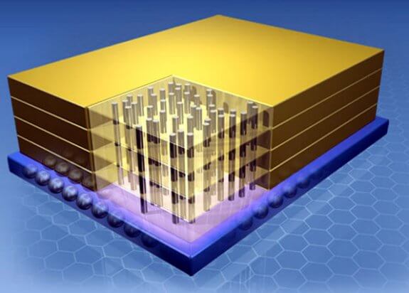
There’s been a lot of buzz around 3D NAND in the past few weeks, sparked by Samsung’s recent announcement that it was commercializing its 3D VNAND technology. There’s also been some discussion (mixed with concern) about how, if at all, 3D NAND might affect the commercialization of TSV-based 3D DRAM technologies, such as Wide I/O 2, High Bandwidth Memory (HBM) the current front-runner, Micron’s Hybrid Memory Cube (HMC).
Herb Reiter provided insight on Samsung’s 3D VNAND here in his recent blog post following his attendance at MEMCON and the Flash Memory Summit, including his thoughts about the relationship between 3D NAND and conventional 3D ICs.

Earlier this month, Cadence’s Richard Goering wrote about the company announcing the industry’s first memory models for five emerging standards. Among those, two target 3D IC architectures: Wide I/O 2, for high-end mobile devices requiring high bandwidth at low power, and HMC for high performance computing. Goering reports “The first Wide I/O 2 devices will probably be 2.5D interposer-based architectures. These take more space than 3D die stacks, but 2.5D chips also have fewer thermal problems, more flexibility to rework connections, and lower costs. Wide I/O 2 is expected to go into mass production in 2015.” He says the much more costly HMC promises speeds of up to 320GBps, 70% less energy per bit than DDR3 and 90% less board space than today’s RDIMMs. “The HMC typically includes a high-speed control logic layer below a vertical stack of four or eight TSV-bonded DRAM dies. The DRAM handles data only, while the logic layer handles all control within the HMC,” writes Goering. Expected production date for HMC is 2014, ironically sooner than the 2.5D Wide I/O 2.
Goering reported also on a MEMCON panel discussion in his post, Promises and Pitfalls of 3D IC Memory Standards, which, in addition to talking about the 3D IC standards, does a great job at explaining the uses for Wide I/O 2, HMC and HBW Memory. Panelist also shared their concerns for interposer cost (Wide I/O 2), thermal management (HMC), and what will drive the leap from DDR 4 to these next-generation technologies.
After absorbing all this recent info on both 3D NAND and 3D DRAM, comments on various posts, and fielding some offline questions, I thought I’d make an attempt to break it all down to the simplest terms, and then see if we can address the relationship between the different technologies.
Defining 3D as it relates to 3D Memory
When these situations arise, as they do every time something gets dubbed “3D”, I find its first to best revisit the definitions of various 3D technologies. I’ve attempted here to break it down with regards to 3D Memory:

- 3D Transistors – Also known as Tri-gate (Intel’s word) and FinFETS, this is 3D at the transistor level. Unlike planar transistors, this design features a third gate in a “fin” structure. Intel was the first to commercialize this technology. (This technology does not really come into play in the 3D NAND, 3D DRAM discussion, but I included it for 3D definition sake.)
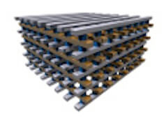
- 3D Chips – Also known as monolithic 3D, this involves stacking transistor layers on top of each other to create a 3D structure. This is where Samsung’s 3D VNAND falls, as well as Toshiba’s 3D NAND offering they call BICS, which stands for bit cost scalable. TSVs are not used in these versions of 3D.
- 2.5D Interposers – In this not-quite-3D configuration, logic die are placed side by side on a passive interposer (silicon, glass or organic) and interconnected using through silicon vias (TSVs). Wide I/O and Wide I/O 2 are interposer-based structures.
- 3D ICs – This is the one we are all most familiar with, and involves stacking at chips using TSVs create 3D IC stacks. This is the technology used for the HMC.
- 3D Heterogeneous Systems – This is also based on using interposers and TSV interconnects to stack different device types on one package. According to Bill Gervasi, memory technology analyst, Discobolus Designs, as quoted in Goering’s aforementioned blog post, heterogeneous systems are “the best hanging fruit in the industry”, because sub-systems of SRAM, DRAM, cache, MRAM, and phase change memory can be combined and when supported with the right software, can provide “phenomenal growth opportunities.”
So with this in mind, its clear that with 3D NAND with 3D DRAM structures, we are not comparing apples to apples. Further, as Reiter notes, the two memory types serve completely different functions. 3D NAND is non-volatile memory, which means it saves information even if the power is switched off, and takes the time to write the data to Flash cells. Alternatively, 3D DRAM (like the HMC) is volatile memory, which only temporarily stores information while the power is on. 3D NAND is expected to take of in the SSD Flash memory market. 3D DRAM is targeted to data servers and mobile devices.
![[err-ad-fallback-title]](http://www.3dincites.com/wp-content/plugins/a3-lazy-load/assets/images/lazy_placeholder.gif)
So why all the concern about 3D NAND pushing out the adoption of 3D DRAM? Likely because there is confusion about the differing applications for each technology.
A Yole report earlier this year looked at the emerging non-volatile memory market, and predicts “Mass storage markets served by flash NAND could begin using 3D RRAM in 2017-2018, when 3D NAND will slow down its scalability as predicted by all of the main memory players.” There is no mention of it replacing 3D DRAM.
However there is a push to develop forms of non-volatile memory to replace DRAM in certain applications. One start-up, Crossbar, recently unveiled a silver-based Resistive RAM technology that the company claims will rival NAND and DRAM (in its current 2D configurations). Bernard Cole wrote about it in embedded.com. This seems to be in pretty early stages of development.
Ultimately, it seems like the commercialization of HMC is likely to beat any of these new developments in non-volatile memory when it comes to actually displacing 3D DRAM. The reality is that currently, NAND and DRAM are different animals serving different purposes. Advancements in both are exciting news and important to achieving next generation goals. What happens down the road remains to be seen, but I think based on what we know today, if TSV-based 3D DRAM is held up by anything, it will be due issues with the technologies themselves, not the advancement of any 3D NAND solutions. ~ F.v.T.


