


This is part of a series of short interviews, based on face-to-face meetings at SEMICON West 2013.
SET is known in the 3D IC world for its high accuracy die bonder for die-to-die and die-to-wafer stacking. The SET Representative in North America (SETNA) has also launched a companion tool, ONTOS7, for the purpose of removing surface oxidation, such as copper oxide from copper pillars. I spoke with the Eric Schulte, inventor of the technology for SETNA, to learn more about why this is necessary and what it lends to the 3D IC manufacturing process.
In 3D assembly, explained Schulte, micro-fine pitch and new bonding metallurgy (such as SnAg capped Cu pillars) requires tighter restrictions on process control. “When you’re trying to bond metal to metal, oxidation and organics can interfere with the bond, and therefore requires higher temperatures and more compression force,” explained Schulte. “Removing surface oxidation and organics allows us to reduce the temperature, force, and time of the bond, which is where the industry has to go to ensure high yields and high thruput for 3D ICs.”
What differentiates ONTOS7’s process from other plasma systems is that it uses atmospheric plasma, avoiding vacuum pumps and load locks. The system performs atomic surface modification by creating active gas-phase radicals inside the plasma head that flow out of the head onto the substrate (chips, wafers, photomasks, PC boards, etc.). Plasma is contained entirely within the process head, never contacting the chip or wafer directly.
For stacked die assembly (D2W) in the 3D IC space, the process is used to prepare both the surface of the chip and the wafer prior to the permanent bond step. Surface preparation adds 2 minutes to the process flow on a die basis, and 5-10 minutes on wafer basis. However, that is offset by the reduction in bonding time and temperature cycling, and enables a metallurgy that allows for 3D tacking at room temperature, followed by an anneal step for the final bond.
At the same time that ONTOS7 is creating ideal surfaces for metal-to-metal bonding, it is also activating the chip surfaces for subsequent underfill. Schulte claims that underfills wick up to 3-times faster with ONTOS7 surface treatment.

Schulte explained that currently, the system is designed for development work to show what can be done with atmospheric plasma. Ultimately, he says this technology enables new paradigms in 3D assembly, allowing for a wider range of acceptable contact metals, and potential for non-reflow assembly, performed at room temperature. For high-volume production, the company plans to produce a 200mm – 300mm wide head to scan a full wafer in one pass. It can either be a stand-alone tool or incorporated into a cluster system.
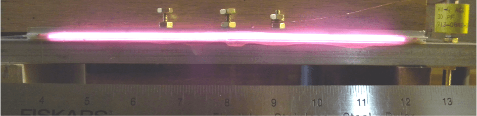 Pictured here is a prototype 200 mm ONTOS7 Atmospheric Plasma Head for incorporation into manufacturer’s cluster systems. Schulte says he anticipates this design to be scalable to 300mm.
Here again is an example of next-stage developments to optimize 3D IC processes for lower cost and meet requirements on next-generation high aspect ratio TSVs that are being developed. ~F.v.T.


