This is part of a series of short interviews, based on face-to-face meetings at SEMICON West 2013.
After my interview with imec’s Ludo Deferm, I met up with Andrew Ho, global industry director, advanced semiconductor materials, for Dow Corning’s Electronic Solutions, to get an update on Dow Corning’s developments in 3D IC assembly materials. I’d previously interviewed Ho’s colleague, J Ranjith John, materials development & integration engineer at Dow Corning, at ECTC 2013, when the company first launched its temporary bonding/debonding solution. So this was just a quick update chat.
The company’s big news is its collaboration with imec to qualify its temporary bonding solution in imec’s process flow. Additionally, Ho says they are working to further enhance the thermal performance of the material to ensure that the chemistry is thermally stable to withstand the high temp environment through the backside process steps, which is a high thermal stress environment.
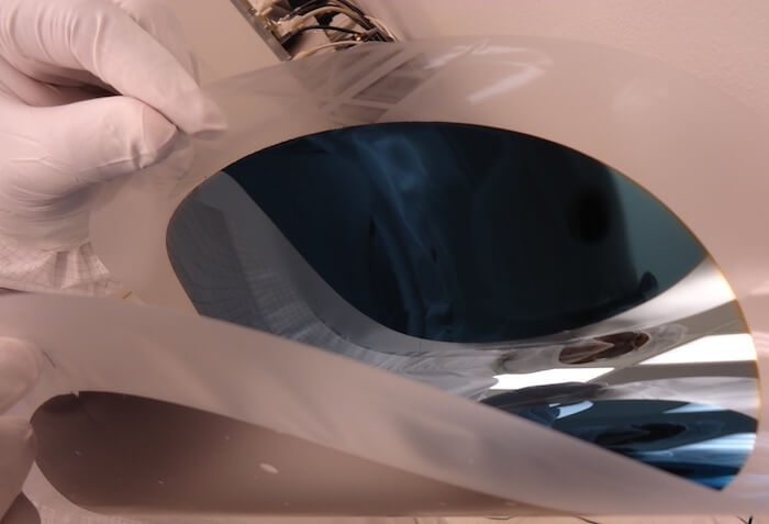
Currently, the material demonstrates good performance in maintaining uniformity of the coating and good mechanical strength. Total thickness variation (TTV) remains low even after backgrinding. Low TTV is important to support reliability in the backside process.
With an eye on high volume manufacturing, where cost of ownership (CoO), yield and throughput is an issue, Ho says Dow Corning is doing its part to lower CoO. “Our solution uses low bond force, which offers the advantage of handling a sophisticated thin wafer,” he explained. Another cost saver is the lack of specialized equipment thanks to the simplicity of the solution. There’s no need for a pre-heat station, the process flow is simple; all of which leads to reduced cycle time. The current goal is to extend the platform to be compatible with all major bonding/debonding equipment partners. “Its about more than low cost of ownership,” noted Ho. “It’s the flexibility we offer to the market.” Currently, the temporary bonding solution can be used for memory to memory, memory to logic, and interposers. The TTV can adapt to microbump applications all the way to a high thickness coating.

Beyond temporary bonding/debonding, what other areas is Dow Corning playing in the 3D IC space? Ho says the mission of Dow Corning is to “explore the power of silicone technology.” They are leveraging a solution in photopatternable silicone technology for 3DIC applications. We’ll be on the lookout for that next. ~ F.v.T.
.