


The Northern California Chapter of the America Vacuum Society has, for years, run a very strong program of ongoing User Group Meetings focused around Plasma Applications, CMP, Thin Films, Junction Technology, and PV. Individually, these worthwhile User Group Meetings, graciously hosted by SEMI at SEMI HQ in San Jose, allow speakers and attendees to focus on, and drill down into, themes of particular interest to Plasma Application Group (PAG) members, for example; one recent PAG meeting was devoted completely to Plasma Processing of Novel Materials, if that’s your cup of tea. (It is mine. Full disclosure: I was NCCAVS PAG chair not so long ago.) 
When the groups come together for a Joint User Group Meeting, as they do once or twice a year, it’s a chance for the community (yes, the NCCAVS User Groups form a community, like 3D InCites does with its readers and contributors) to bring all its powers to bear examining a particular subject from multiple angles.
Just think how much sense it makes to consider 3D Packaging from a CMP perspective and from a plasma etch perspective, with a little thin film flavor thrown in for good measure, all in an afternoon. Add to that an invitation that says “All are welcome. Admission is free. Just show up.”
Sound good? It was indeed at the June 2013 NCCAVS Joint User Group Meeting on 3D Packaging, June 11, 2013. which filled the conference room at SEMI HQ with about 80 attendees, and featured five distinguished speakers who presented these informative talks:
- “Thermal and Stress Management for 3DIC Performance and Reliability” (Valery Sukharev, Mentor Graphics)
- “Cooling Three-Dimensional Integrated Circuits Using Power Delivery Networks” (Hai Wei, Stanford University)
- “Overview of CMP for TSVs” (Rob Rhoades, Enteprix)
- “Considerations When Selecting a Wafer Level Bonding Process” (Garrett Oakes, EVG)
- “3D Packaging for Memory Applications” (Ming Li, Rambus).
“Thin is in,” said Valery Sukharev in his lead-off talk, noting how thin silicon devices (50µm thin, or even 20µm) are all the rage these days for deployment in applications like smartphones, whether the devices feature 3D packaging or not.
In the past, said Sukharev, reliability problems associated with new technologies came from the introduction of new materials, like low-k dielectric materials with their weak mechanical properties, or from materials like copper, which can be poison to silicon devices.
Now though, in the 3D Age, it’s die thinning, with or without through silicon vias (TSVs) for 2.5D or 3D IC, that’s introducing new areas of device reliability concern. Stress in thin wafers, and thermal effects in thin, or thin stacked die, both require that new modeling tools be applied before first silicon is run.
 Regarding the interaction of thin devices, stress, 3D IC, and wafer bumping, Sukharev said “Bumps are an elephant in the wafer stress room.” As a result, some of the old electromigration reliability models have become inadequate, and in the 3D Age we now need to account for warpage-induced stress, bump-induced stress, TSV-induced stress, etc., along with Chip-Package Interaction (CPI), in addition to everything else the models had to account for before very thin die and 3D IC came along.
“New technology brings new stress, both psychological and technological,” noted Sukharev, (as GLOBALFOUNDRIES is well aware, based on its 3D IC talk at ASMC 2013.)
The appropriate response for Mentor Graphics means deploying new package-scale simulation models, new die-scale simulation models, and new layout-scale (with feature scale resolution) models in order to do things like look for hot spots using thermal modeling, under conditions where the device/module/smartphone is variously being used to make a phone call, send a text, or take a photo. That’ll verify the designs such that there’ll be no chance of developing skin temperatures that would make you want to drop your phone like a hot potato (if the thermal overloads already hadn’t caused the embedded devices to fail too soon in the first place).
Are you wondering, like someone I saw posted on LinkedIn this week, about how to manage heat in 3D IC applications? For Hai Wei, Stanford, the answer is to use the power distribution network interconnect layer running through thin 3D IC die to bear the lion’s share of heat management, rather than relying on the (less robust) thermal conductive properties of thin silicon itself. When modeling heat management, as alluded to also in Sukharev’s talk, Wei said it’s a must to account for the many different applications a single 3D IC might be running (talk, text, photo) in order to avoid any unpleasant thermal surprises. Wei also introduced the idea of parallel 3D IC processes, in which die are added to die (what I always think of when I think of 3D IC); as well as sequential 3D IC processes, in which additional active layers are added directly on top of base-layer devices without using any kind of bonding scheme – just building up.

I think I need to chew on that a little more before it sinks in for me.
“2D scaling is reaching the fundamental limits of physics (and of balance sheets),” said Rob Rhoades, Enteprix, and CMP is there to support, in several ways, the move to the 3D IC dimension. There are several uses for CMP in 3D IC processes: most notably removing overburden copper (something like 45µm of it) after TSV Cu via fill plating, but also for removing wafer backside bulk silicon (something like 30µm in Rob’s example) using CMP during TSV reveal. These are quite different missions for CMP than it typically sees for standard damascene applications, and has therefore required extensive optimization of CMP slurries, emphasizing high rate slurries, and also emphasizing the optimization of various selectivities to underlying materials during the polishing steps. There are also schemes for two-step TSV reveal processes, where CMP of the backside silicon is performed after the bulk of the silicon has been removed in either a wet or a dry silicon etch process. Why do one over the other? There may be certain cost advantages to the two-step process, depending on what set of CMP and silicon etch processing tools are already owned by the wafer fab performing the work.
Per Garrett Oakes, EVG, for 3D IC bonding it’s the Cu-Cu thermal compression bond that is most popular among the many different kinds of wafer bonding available.  Garrett also showed pages and pages of flowcharts demonstrating “best known practices” developed by EVG during its years of work on both temporary and permanent wafer bonding; an impressive testament of how today’s 3D IC unit operations (wafer bonding, deep silicon etch, CMP, etc.) have benefitted from years of prior work performed by EVG, and others, during their work in MEMS device fabrication and packaging, from which much of today’s 3D IC manufacturing processes have been ported.
Plus ca change, plus c’est la meme chose.
Except the wafers got bigger.
Before leaving the subject of 3D Packaging there is one more talk to consider; one by Ming Li, Rambus, on High Bandwidth Memory (HBM) based on 3D IC / TSV architectures. 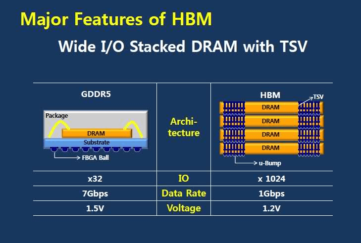 Similar to the Hybrid Memory Cube concept promoted by Micron and others, HBM, as promoted by Rambus, tilts the playing field in favor of making a wide I/O memory architecture using stacked DRAM die with TSV interconnects between the die in a double-sided flip-chip package with a processor on top and stacked DRAMs on bottom. In this middle-ground approach between traditional package-on-package, on-PCB solutions and pure-3D integration, the processor interfaces with memory directly through the package, which yields very high I/O density and low-loss interconnect paths, along with thermally decoupled processor and memory devices. It’s a neat solution to some of the thermal issues that surround 3D IC. On a practical note, Ming said the fab work for the Rambus HBM is being performed by Tezzaron, who have already gained quite a name for themselves in the field of stacked memory die, this being yet another of recent mentions.
Before ending this summary a word goes out to acknowledge Lucia Feng, Kapila Wiejekoon, and Hok-Kin Choi, volunteers all with the NCCAVS, who organized, and co-chaired, this 3D Packaging Joint User Group Meeting. Good job all, particularly Lucia. From Petaluma, CA, thanks for reading. ~ PFW
PS: Information on the NCCAVS User Groups can be found here.


