


Those of us following 2.5D and 3D ICs have been holding our breath waiting for test solutions to appear amidst all the controversy surrounding whether or not partial testing of 3DICs just adds cost or whether it adds value. I spent some time talking to Bob Chartrand, director of sales and service for North America and Jim Quinn, VP Global Sales and Marketing at the Multitest booth at ECTC 2013 (Las Vegas) to get their perspective as a test solutions provider, as well as learn about their efforts in partial stack test for 2.5D and 3D IC. What they had to share was pretty compelling.
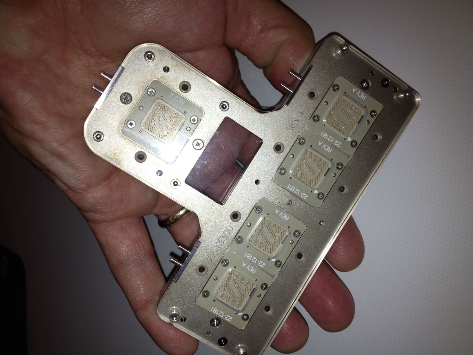
If you think test solutions don’t exist yet in the industry, you’re wrong. According to Chartrand, Multitest’s InStrip3D Plug& Yield® solution is the “only true in-process testing tool on the market” and the company is working in production with a customer who is a major player in the industry focused on mobile SoC (Figure 1). At APEX IPC 2013 (February 19, 2013, San Diego), the InStrip3D Plug& Yield® solution took home the 2013 NPI Award from Circuits Assembly magazine in the category of Test & Inspection – Functional Test.
This in-strip platform is used to test partially built 2.5D or 3D TSV interposer stacks. It essentially tests the substrate silicon with some of the die placed on it. If there is a failure during the in-process test, the tool’s x+plus+one configuration makes it possible to retest one die one the load board. It functions like a prober, said Chartrand. With probe-like accuracy, the strip is plunged up to the contact site, where tiny pins touch the device and perform the test. The tool was originally developed for a high volume manufacturing (HVM) MEMS platform, where Multitest learned how to support tiny, delicate devices. “3D devices are large, compared to what with MEMS,” he noted.
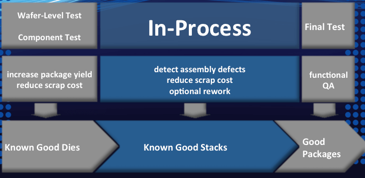
Quinn explained that the tool is currently being used to test 3D heterogeneous devices. The idea to test the logic and have a “known good stack” (logic on interposer in any combination) before costly memory stacks are introduced to the device. This in-process testing allows for possible rework before adding the memory stack. “In this way, test becomes process control,” said Quinn, adding that this is a change in the assembly process flow to put test into the assembly area (Figure 2).

Partial test adds value, he noted, because of the high bill of materials for 3D heterogenous devices with 3D TSV memory stacks. Rather than tossing an entire defective device, we now have the ability to determine “known good stacks” before integrating a memory device on a defective stack. “It’s too expensive NOT to test on an interim basis,” says Quinn. “The challenge is convincing people that in-process testing is necessary. One customer has made the decision.”
After hearing Quinn’s argument, I’m convinced. I suspect more customers will follow. ~ F.v.T.


