


Are you familiar with the Japanese custom of cherry blossom viewing? “Hanami (花見, lit. ‘flower viewing’) is the Japanese traditional custom of enjoying the beauty of flowers, ‘flower’ in this case almost always meaning cherry blossoms (‘sakura’) or (less often) plum blossoms (‘ume’).” (Source: Wikipedia.)
But what, you may ask, does cherry blossom viewing have to do with 3D IC?
I was in San Jose last week at SPIE Advanced Lithography 2013 attending the 2013 Advanced Lithography Exhibition, hoping to catch whatever was being said about 3D IC applications by exhibition vendors who were otherwise advertising such technologies as immersion, double patterning, e-beam, EUV, optical/laser, and RET lithography (naturally), materials and chemicals, resist materials and processing, and nano-imprint systems for IC and chip fabrication.
Mentions of 3D IC, or of Through Silicon Vias (TSVs), in either the exhibition guide or in the technical program itself were pretty sparse; I saw that Eric Beyne, imec, was speaking on “The Advent of 3D System-on-Chip Integration,” and that Victor Vartanian, SEMATECH, had a paper on “TSV Reveal Height and Bump Dimension Metrology by the TSOM Method,” but that was about it. (Readers, please fill me in if there was indeed more.)
I just figured I would try my luck walking the show floor to see whether I could spot a 3D IC blossom or two poking out in the garden of booths.
 Walking toward the Lithography Exhibition at the San Jose Convention Center under a canopy of San Jose street tree blossoms, and then entering the hall to see the largest contingent of Japanese attendees I have seen at any recent conference I’ve attended, I thought maybe it was appropriate to think about the advancement of 3D IC in the semiconductor industry to be something like the cherry blossom front that advances over Japan each Spring.
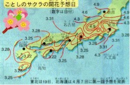 In Japan there’s a map published for tracking the advancing blossom front, there’re updated forecasts for when blooming will happen, you see the early buds, and then, boom, blossoms everywhere.
Well the cherry blossoms were out in San Jose last week, and here are a few of the 3D IC bud sightings I made at the SPIE 2013 Advanced Lithography Exhibition.
Brewer Science was seeing lots of booth traffic over some combination of their offerings for specialty materials, equipment, and process solutions for applications in semiconductors, advanced packaging/3-D ICs, MEMS, sensors, displays, LEDs, and printed electronics. Alex Smith from Brewer was heavy in the mix, busy enough with customers I never had the chance to speak at length with him about his thinking regarding 3D IC, and what kind of action Brewer was seeing at Advanced Lithography over 3D IC processing. Maybe their buzz was over the new generations of ARC® and OptiStack® materials Brewer is promoting? I’ll have to get Alex aside sometime soon for a follow-up to confirm.
Over at Nanometrics, I was able to speak with the very engaging Dr. Brennan Peterson, Director, Strategic Product Marketing, drawn to the Nanometrics booth as I was by the display promoting Nanometrics’ inspection products and their use in 3D IC.
Nanometrics’ UniFire tool is said to offer customers a broad range of features to control micro bump, redistribution layer(s), and TSV patterning, including critical dimensions (CD) measurements, registration, depth/height/profile, and wafer bow/shape and film thickness in 3D packaging applications. Adding to those capabilities, Nanometrics also finds process induced defects with its SPARK system, an ultra-fast inspection tool capable of finding defects associated with TSV formation, as well as wafer bonding, thinning and backside processing.
All good, but it was the free-ranging discussion I had with Brennan on 3D IC topics that really made me think Nanometrics knows what’s going on with the state of the 3D IC blossom front. (Me: “Brennan, you’ve really given a lot of thought to these 3D IC topics.” Brennan: “It’s my job to think about that.”)
Nanometrics, like many of the other vendors in the 3D IC space, has production tools ready now for the 3D IC party. (Can you say that EUV?) But why even do 3D IC when PCB is still a good alternative? Why do 3D IC stacked memory when embedded DRAM, as promoted by IBM and others, is a good alternative? Why do full-on 3D IC at all when 2.5D silicon interposers are a good alternative?
Brennan asks “What are the applications that make the 3D IC business story fly?” There are answers at the high end of the business, but what about at the volume end?

Good question Brennan.
On the other hand, I hear the cost of implementing 3D IC process modules looks like a pretty reasonable bet to make compared to taking an expensive flyer on EUV lithography once you start backing fast horses. (Is this kind of thinking apostasy at an Advanced Lithography symposium?)
You can fill a whole 3D IC stable before you’ve got a single EUV pony saddled and ready to go.
I spotted a TSV bud at the DNS Electronics booth, where Ian Winch, Senior Product Engineer, helped me understand DNS’ approach to 3D IC applications, which is to extend the capabilities of their existing tools, with their already-proven production manufacturing track records, to the TSV arena.
Good idea that.
And I literally stopped to admire the blossoms at Tokyo Ohka Kogyo (TOK) America, Inc. Their booth floral arrangements reminded me of tradeshows in Japan, fitting for this American branch of a Japanese parent. TSV applications figured pretty prominently in the booth display, and I have a follow-up on tap with Amy Palesko, Business Development Representative, TOK America, Inc. to find out more about the TENTING process in TSV formation.
More for me to find out from Rudolph Technologies, which, Ardy Johnson, Vice President, Corporate Marketing and Product Management, was eager to point out, has a newly released 2X wafer stepper on the market designed for a variety of advanced packaging applications, including TSV.
Ardy, I’ll be calling you.
Finally, I made a mental note the first time Tezzaron and 3D IC were mentioned to me in the same sentence as I asked about commercial examples of and prospects for 3D IC here at the Lithography Exhibition; after hearing the same mention repeated several times my conclusion is it seems like everyone in the 3D IC capital equipment and materials business is keeping pretty close track of Tezzaron as being the key harbinger of the coming 3D IC cherry blossom bloom.
With many more blossoming trees to follow.
From Petaluma, CA, thanks for reading. ~ PFW


