


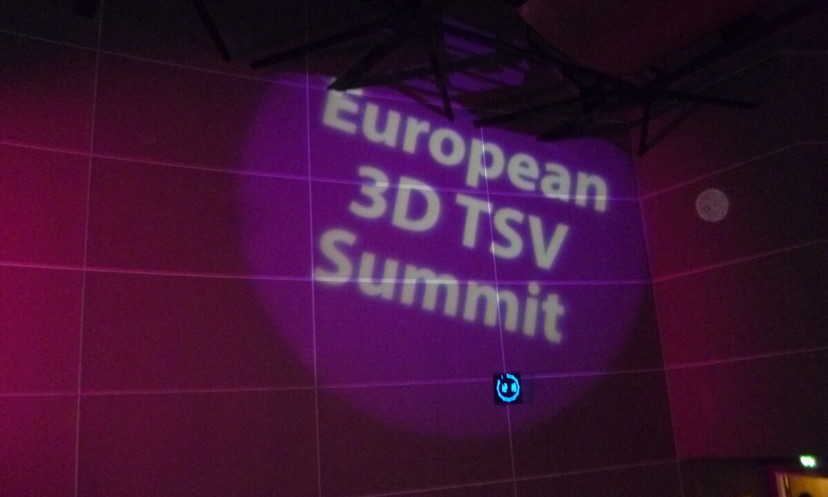
Here I am, on my way back from Minatec Campus in Grenoble, France, where I attended SEMI Europe’s premiere European 3D TSV Summit. It was such a whirlwind few days, jam-packed with quality presentations demonstrating recent progress in all things TSV by the semiconductor manufacturing community and fabulous meals with industry colleagues and friends that this flight home is the first time I’ve had to write about it (unless you count the nuggets of information I posted via Twitter found here at #3DTSVSummit.)
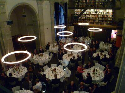 There’s no doubt about it, SEMI Europe pulled out all the stops to show its 300 guests from 20 countries that Europe is serious about 3D TSV commercialization. And they did it with a flair that the French have mastered. I mean, where else will you sip wine during the lunch break and dine on terrine de fois gras, petite fillet, potato gallette, and a selection of Alsatian cheeses at a Gala dinner held in a centuries-old convent?
One thing is clear; we’ve certainly come along way from the early days of proof of concept presentations. Since 2005, when I began following emerging technologies that have become mature processes in 2013, I have learned a lot thanks to conferences like this one. And along the way, I got to witness 3D TSVs come of age.
As imec’s Eric Beyne talked about in his presentation on Tuesday, in the beginning there were a variety of process flow solutions being developed. Now as high volume applications emerge, it becomes clearer which technology works best for each, and the field has narrowed considerably. He calls it “technology convergence”, which he says will help Cost of Ownership (CoO).
Throughout the presentations, a common thread emerged: The technology blocks are ready for both 2.5D and 3D applications. But as it stands, the only products that will currently benefit are those that can bear the high sticker price. Others will have to wait for the processes to be optimized to lower CoO. Ron Hoemueller, of Amkor, showed a chart that put interposer wafer prices in 2014 at $2900/wafer, which will need to be reduced to $750/wafer to be able to justify putting them in “value markets”. We won’t see prices like this until about 2016.
However, for high-end products like FPGAs, 2.5D technologies have provided lower cost, higher yielding solutions than SoC scaling can. Suresh Ramalingam, of Xilinx, explained that 2.5D interposers buy us connectivity, capacity and crossovers. Interposers provide a high-density wiring platform with low latency, which results in 100x efficiency over conventional methods in terms of bandwidth/watt. Multiple die slices offer capacity beyond what Moore’s Law can provide, with a fast yield ramp over single monolithic die. Finally, they offer the ability to mix functions (memory, analog, and processor). “It still looks like an SOC, but how we build it is like a crossover SOC.” Said Ramalingam.
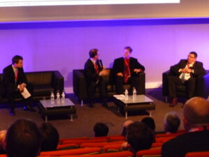 Business models were another central topic of discussion, particularly with the panel discussion, 3DIC –TSV Ready for HVM?, co-moderated by Lionel Cadix, of Yole Developpment and Yann Guillou, of SEMI Europe, and featuring on the panel, ASE’s Brad Factor, Ron Huemoeller, and Heinz-Peter Wirtz, of STATS ChipPAC.
With regard to a question on remaining technology challenges, Huoemoeller reiterated that technology bricks are ready (with the caveat that there are still thermal issues to be sorted out for pure 3D). Even with everyone’s nemesis, temporary bond/debond (TB/DB), long-time considered the bottleneck, Amkor is reportedly achieving 100% yield. The cost of the wafer support system continues to be a sticking point, however. Wirtz emphasizes the thermal issue, saying that the high junction temperature resulting from putting a high power processor next to the memory could be a major issue and needs to be worked out.

On the question about business models, all agreed that a collaboration model is preferable, although there’s still concerns about liability and “ownership.” (Of course, we were only getting the OSATS perspective, because Jon Greenwood of Globalfoundries, who was supposed to provide the pure-play foundry perspective, was delayed due to weather. But he concurred the next day during his keynote address.) Brad Factor explained that with memory and processors being assembled together, it becomes complicated. The most logical solution is a ‘consignment model’ where the owner of the module pays the bill. Wirtz agreed that the OEMs should take the leadership position. “They’re the ones who have access to memory at the right pricing. With that step, they can enter the mass mobile market and drive the price down,” he noted. Quoting his ASE colleague Rich Rice, Factor cited Samsung as one player who can do it all, since they manufacture memory, processors and do packaging. “If they start doing it, others will figure it out quickly,” he said.
Finally, as this summit was intended to demonstrate Europe’s activities in 3D TSVs to the world, the discussion turned to the role of Europe in the TSV market. While Europe is clearly the R&D hub for the technology, and maintains a strong leadership worldwide in semiconductor equipment manufacturing, as noted by Hoemueller, there seemed to be some concern on the manufacturing end, without a strong Nokia or Ericssion to lead the charge. Wirtz pointed to the strong consortia involving ST Microeletctonics, Leti, imec and Fraunhofer, and the potential for 3D in automotive, industrial and medical markets.
I asked Heinz Kundert, President of SEMI Europe for his perspective on the drive back to Geneva. He disagreed with the panel’s assumptions, and cited many manufacturing opportunities to support TSV in Europe such as GlobalFoundries in Dresden, ST Micro, and Infineon; “All device makers regardless of applications are looking into TSVs.” He explained. This includes automotive, MEMS sensors, power electronics, and other TSV applications that aren’t 3D. He explained a growing interest in Russia for semiconductor device manufacturing, and that they don’t want the hassle of getting chips from “the outside.”
Kundert also talked about a growing megatrend in Europe, as well as the US, to bring manufacturing home. This is why he would like to see the EU commission help ease business costs in Europe and make it more competitive here. He said it’s no longer cost-effective to manufacture offshore when you consider the cost of technology transfer and paperwork for sending ex-pats overseas. “An engineer in China is more expensive than an engineer in Germany,” he noted, adding that productivity is lower than the salary increase. “We go to Asia because it’s a big market, not because of low labor costs.”
All in all, it was a great first 3D TSV Summit. I’m just barely digging into the information I gathered. I haven’t even touched on the presentations from equipment and material suppliers, who had lots to say with regard to processes optimized to reduce cost. That’s what I’ll be bringing you next. In the meantime, save the date for next year’s event, already planned for January 21 and 22. I’m hoping to be invited back to cover it for 3D InCites. ~ F.v.T.


