


Up until recently, I really hadn’t paid much attention to the the intricacies of memory types required to satisfy the plethora of computing needs from today’s PCs to tomorrow’s data centers and mobile devices. I had a general understanding of caches and main memory, and the increasing need for shorter interconnects and wider bandwidth. And I knew that one of the big drivers for 3D memory solutions was the fact that today’s memory technologies can not keep up with the exploding memory requirements driven by data centers and mobile devices that are chewing up memory bandwidth faster than we can extend it.
But it’s actually even more dire than that. Did you know that the technology required to meet the needs of cloud computing by 2016 doesn’t even EXIST? Or at least it didn’t back in March when Dr. Raj Jammy, VP Materials and Emerging Technologies, SEMATECH, said as muchduring a presentation he gave at the Memory + conference in Tokyo. Here’s why: In addition to the memory demand, there’s the “instant on – instant connectivity” expectation of consumers. (Seriously- I just sent my daughters off to college and one of the biggest stressors expressed so far is the crappy internet connection in the dorms because so many students are trying to access the same wifi connection with all their devices.) Additionally, sensing technologies that make devices smart and allow for human interaction are increasingly critical.
It’s important for computing to remain server based, explained Jammy, so cloud computing is expected to grow to a $44.2B market by 2013. Power requirements are expected to reach exascale proportions (1018, 1500MW with a 3.6 petabyte memory requirement) by 2016. What is required, Jammy explained, is a new class of memory that has the multilevel storage, density and cost of NAND, but is faster with improved functionality and reliability. Further, he said future memory will not be based on electron storage like NAND and DRAM, but will be resistance change based technologies. And to complicate things even further, we’re no longer just talking about stand-alone memory, but systems-on-chip (SoCs) that integrate the processor, with various memory components (DRAM, SRAM, non-volatile memory) in one tidy package.
Luckily, the memory companies (SanDisk, Toshiba, SK hynix, Micron) are all working on solutions, and whether it’s achieved by stacking die using TSVs (3D ICs) or building up layers (monolithic 3D) it’s almost inevitable that the next generation of memory to be manufactured will move into the 3rd dimension.
3D NAND
The 3D memory flavor of the month (and particularly since Applied Materials announced it’s new etch tool in July and started writing about it) is 3D NAND, which is manufactured using a monolithic 3D approach. There’s an informative blog along with a video posted here on Applied Materials’ website that gives a good explanation. 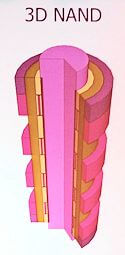
Additionally, Richard Goering, of Cadence, blogged about various 3D NAND structures in a recent blog post, New Memory Technologies Challenge NAND Flash and DRAM, summarized from the keynote delivered at this year’s Flash Memory Summit. For an even more detailed look at various types of 3D NAND and other phase-change memory technologies in development (based on SK hynix’ roadmap) is Goering’s post in the Denali Memory Report last week.
3D BiCS and 3D ReRAM
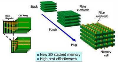
3D memory being developed at Toshiba includes bit cost scalable (BiCS) and Crosspoint 3D (also known as 3D ReRAM). The process for manufacturing BiCS 3D memory is simple. Stacking the memory is a sequential process in which the three steps – stack, punch-plug – are performed simultaneously at low cost. 3D resistive random access memory (ReRAM) is being developed simultaneously with BiCS, in collaboration with SanDisk. The structure is 3D, but the resistive device is located in the cross-section. One is to increase resistance, and one is to reduce resistance. (Below is an explanation of BiCs technology, pulled from this presentation by Jeff Ohshima, during the GSA Memory +Conference)

3D ICS
On the 3D IC side for memory, the poster child is Micron and Samsung’s Hybrid Memory Cube (HMC), consisting of DRAM stacks interconnected with TSVs and mounted on a logic die. This technology ultimately aims to provide a viable solution for hetreogeneous integration.
Earlier this week, SemiWiki’s Paul McLellen wrote a somewhat detailed report on the model HMC, based on a presentation given at DesignCon 2012. One of the key takeaways of this modeling, according to McLellen, is that physically partitioning the device simplifies design, modeling and simulation.
My main goal in pointing readers at all this information is to once again emphasize (because some things can’t be stressed enough) the numerous technologies that are emerging to exploit the third dimension, and to make sure we understand the differences in manufacturing processes. 3D NAND and 3D DRAM are structurally completely different, and also serve different market spaces. Both will be vital to fill the memory gap that will only continue to widen unless solutions are found. ~ F.v.T


