


There’s been lots of news lately about the transition to 450mm wafers, and I’m wondering, is it only me, or are there others who are amazed at how little mention there is on its impact in the assembly and packaging world. It’s like the front-end has forgotten that the back-end has wafer level processes too! Furthermore, the back-end equipment manufacturers don’t have the same profit margins as front-end equipment suppliers, making the cost of development an even bigger deal for them. And when it comes to 3D ICs, there are already gigantic issues with handling ultra-thin 300mm wafers; I can only imagine what the tool manufacturers will be facing with 450mm wafers.
Last week, SEMI introduced a new 450mm information portal, 450mm Central to help the communication efforts as efforts ramp up to the wafer transition. As Jonathan Davis was quoted in the press release, ”Robust communication throughout the supply chain is essential for a cost effective wafer size transition.” This portal is designed to be an information clearinghouse to keep the industry informed on important news and perspectives on 450mm wafer processing. There’s one thing 450mm and 3D ICs have in common; the impact on the entire infrastructure is inspiring collaboration and cost-sharing to get the things going in both areas. It does seem that there are alot more players in the 3D game than in 450mm wafers.
I took a tour of the new portal, and was very happy to see an article by Semi Europe’s Yann Guillou, (who also happens to be on the 3D InCites Advisory Board) addressing back-end challenges as a result of the wafer transition. He reported on a recent workshop held in Grenoble Beyond 300mm: Packaging Challenges and Opportunities for 450mm Wafers and Panel Scale Solutions during which players from both the front-and back end gathered to discuss areas of overlapping concern, with a particular focus on package and assembly developments. However, I was disappointed to only read about progress with Fan-Out WLP, embedded technologies, which are based on ‘reconstituted’ or rebuilt wafers and/or panels; and enabling 2.5D integration.
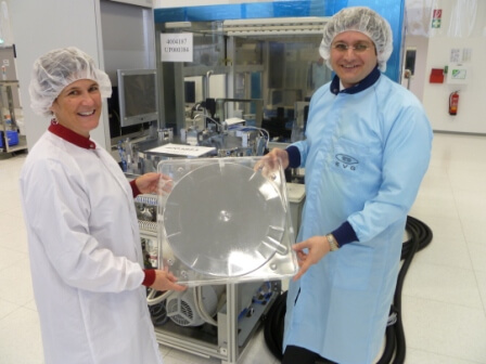
Apart from EVG’s 450mm bonding tool (above) developed in conjunction with Soitec for SOI wafers, and a “clear internal roadmap for 450” at EVG, not much else was said with regards to the implications for 3D ICs. (Does anyone know of any other tool suppliers to the advanced packaging market who are working on their 450mm tool sets?)

Oh and by the way, today’s Digitimes reported that the date for mass production of 450mm (18 inch) wafers has been pushed out to 2018 from the original 2016 date, despite investment from Intel, TSMC and Samsung, and equipment developments at ASML. So I guess we still have time to worry about the implications for 3D. In the mean time, we’ve got plenty to concern ourselves with getting 3DICs to volume manufacturing. After that, maybe then we can address the 450mm challenges, although I still think it would make the transistion easier if they were addressed along the way! ~ F.v.T


